
Copper Clad Laminate: Types, Properties and PCB Selection
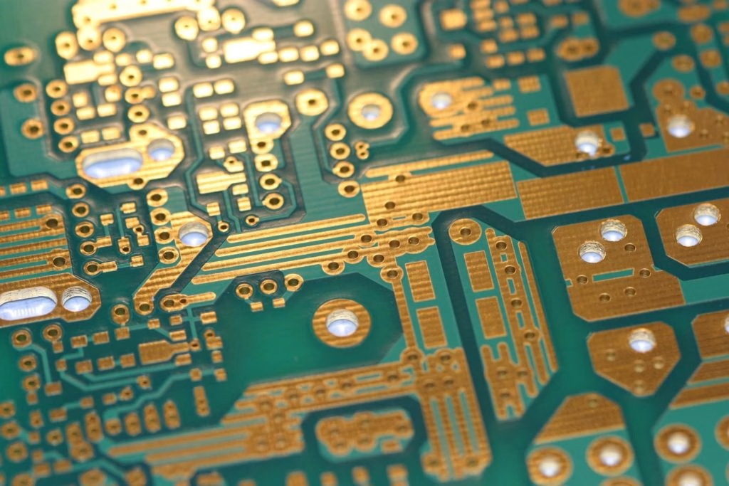
Table Of Contents
Copper clad laminate (CCL) is a copper-bonded insulating base material used to manufacture printed circuit boards. Choosing it involves the dielectric system, reinforcement, copper foil and manufacturing construction together. The name FR-4 alone does not fully specify a PCB material.
1. What Is Copper Clad Laminate?
A CCL combines a cured dielectric substrate with copper on one or both sides. In conventional rigid boards, glass reinforcement and a thermosetting resin form the insulating structure. Other constructions use different resins, reinforcements or unreinforced films.
The fabricator patterns copper into circuitry. A multilayer PCB combines patterned cores, bonding layers and copper according to an approved stackup. CCL is a starting material, not the completed PCB and not the solderable PCB surface finish.
2. How Are CCLs Classified?
- By mechanical construction: rigid laminates and flexible copper-clad materials serve different bend and support requirements.
- By dielectric system: glass-reinforced epoxy, polyimide and specialized high-frequency systems have different processing and electrical behavior.
- By reinforcement: woven glass, paper and composite constructions are not interchangeable simply because thickness matches.
- By construction: specify dielectric thickness, copper thickness, sidedness and tolerances explicitly. Do not assume a universal 0.5 mm boundary defines every supplier’s thin-laminate category.
FR-4 copper clad laminate describes a material family, not one fixed Dk, Tg or temperature capability. Specify an approved manufacturer and grade, applicable material requirements and an alternative-approval procedure.
3. What Makes a Suitable CCL?
A suitable material meets the electrical, thermal, mechanical and processing needs of the actual board. Appearance matters, but visual inspection cannot establish every reliability property.
| Property | Why it matters | What to verify |
|---|---|---|
| Dk and Df | Impedance and dielectric loss | Frequency, test method and actual glass/resin construction |
| Tg | Change in material behavior near glass transition | Measurement method; not a maximum operating temperature |
| Td | Thermal decomposition behavior | Specified mass-loss criterion and method; not a reflow setting |
| Z-axis CTE and expansion | Stress on plated interconnects during heating | Temperature range and actual stackup |
| Peel strength | Copper adhesion under defined conditions | Foil type/thickness, conditioning and test method |
| Moisture and insulation behavior | Electrical reliability under exposure | Environmental conditions and qualification evidence |
| Thickness and dimensional stability | Stackup, registration and fabrication yield | Tolerances, construction and processing controls |
Compare equivalent measurements. A Dk value at one frequency or obtained by one method may not be interchangeable with another supplier’s design value. For controlled impedance, work from the fabricator’s proposed construction and modeling assumptions.
Do not claim that every halogen-free material has worse peel strength or every conventional FR-4 has poor thermal performance. Those properties depend on the grade and construction. Manufacturer data such as Isola’s laminate and prepreg documentation provides a better basis than generic good/bad tables.
Where an IPC material specification is required, agree its revision and relevant material designation with the supplier. The IPC test-method collection is IPC-TM-650, not IPC-TM-655. A test-method reference alone does not establish that a material or finished board is qualified, and no unverified factory compliance claim is made here.
4. What Is PCB Prepreg?
PCB prepreg is reinforcement impregnated with partially cured resin, used as a bonding dielectric during multilayer lamination. Under a controlled press cycle the resin flows and cures. A cured core and a sheet of prepreg therefore have different roles.
Glass styles such as 1080, 2116 and 7628 describe reinforcement constructions; they are not complete prepreg specifications. Resin content, resin system, flow behavior, cured thickness and processing limits must also be defined. Not all bonding films or high-frequency dielectric systems use the same glass-and-epoxy construction.
Specify the proposed material combination rather than mixing core and prepreg families without approval. Store and handle prepreg according to the supplier’s shelf-life, temperature and humidity instructions. Uncontrolled exposure can change processing behavior.
Isola’s laminate and prepreg manufacturing guide explains the distinction. For purchasing, compare the exact construction and availability; thinner glass is not a universal price rule.
5. What Is Copper Foil?
Copper foil provides the conductive layer bonded to the dielectric. Electrodeposited and rolled foils are broad manufacturing categories, with treatments and variants inside each. Select foil for the specified electrical, adhesion, fabrication and flex requirements rather than relying on an unsourced class-number table.
For a copper foil PCB review, record nominal starting thickness, foil type, treatment, surface roughness information and finished-copper requirements. Plating can change the finished copper thickness, so starting foil and finished conductor thickness should not be treated as identical.
At high frequencies, roughness and the copper/dielectric interface can influence conductor loss. Compare the relevant roughness metric and material construction. Rolled foil is not automatically the correct choice for every board. Rogers’ copper-foil reference illustrates the differences between foils used with specific circuit materials.
6. Material Selection Trends and Practical Review
Lead-free assembly compatibility, lower-loss interconnects and material-disclosure requirements are separate selection questions. Halogen-free is not a synonym for lead-free soldering compatibility. Do not infer either electrical performance or whole-product compliance from one material label.
For thermal demands, review the complete material data and proposed fabrication and assembly sequence. High Tg alone cannot guarantee survival through repeated reflow or a particular operating life. For high-speed or RF work, select the dielectric and copper construction together.
Material review checklist
- State the application, operating environment, reliability requirements and assembly thermal sequence.
- Provide layer count, finished thickness, copper requirements, controlled-impedance targets and critical geometry.
- Agree the exact laminate/prepreg grades, construction, test conditions and relevant specification revision.
- Review fabrication compatibility and availability with the supplier before accepting a substitute.
- Document material traceability and the verification required for the finished board.
Is copper clad laminate the same as prepreg?
No. A conventional CCL core is a cured copper-clad structure; prepreg is a partially cured bonding material used during lamination.
Is all FR-4 equivalent?
No. Grades differ in resin chemistry, thermal and electrical behavior, reinforcement and construction. Approve alternatives against the actual requirements.
Does higher Tg always mean a better PCB?
No. Tg is one property. Consider expansion, decomposition behavior, dielectric performance, processing and qualification together.
What should I send for a material review?
Send the fabrication drawing, proposed stackup, operating conditions and material restrictions. For a combined build, include the BOM and assembly sequence in your PCB assembly enquiry. Request a project-specific review before replacing an approved PCB laminate.
Contact Us
Phone: +86-18123905375
Email: sales@assemblepcb.com
WhatsApp: +86-18123905375
Wechat: +86-18123905375
Free Queto
Latest Blog


Table Of Contents
Contact Us
Phone: +86-18123905375
Email: sales@assemblepcb.com
WhatsApp: +86-18123905375
Wechat: +86-18123905375
Free Queto
