
Mastering High-Density BGA & QFN PCB Assembly: A Complete Guide to X-Ray Inspection and Defect Control

Table Of Contents
1. Introduction: The High-Density Challenge
In today’s rapidly evolving electronics landscape, devices are becoming smaller, more powerful, and increasingly complex. This miniaturization trend drives the widespread adoption of high-density integrated circuit packages such as Ball Grid Array (BGA) and Quad Flat No-lead (QFN) components in modern PCB assembly (PCBA). While these packages offer major advantages in performance and footprint, their intricate designs create real challenges for surface mount technology (SMT) assembly and quality control. Ensuring reliable solder joints — especially those hidden beneath the component body — is essential for long-term product functionality and reliability.
This guide explores the critical technologies and best practices required to achieve flawless high-density BGA and QFN PCB assembly, with a particular focus on the role of X-ray inspection for PCBA in guaranteeing solder joint quality. Whether you are evaluating a contract manufacturer or refining an in-house SMT line, understanding these fine-pitch component assembly techniques is essential for reducing defects and improving first-pass yield.
The stakes are high: a single defective solder joint can lead to product failure, costly rework, or even safety issues in the field. Manufacturers must therefore apply rigorous process control across the entire assembly workflow — from precise solder paste deposition to meticulous post-assembly X-ray inspection. For any company operating in advanced electronics manufacturing, mastering these techniques isn’t optional; it’s a competitive necessity.
2. Understanding BGA and QFN Devices
Before diving into the assembly and inspection technologies, it’s crucial to grasp what makes BGA and QFN packages unique — and why they demand specialized PCBA quality control.
Ball Grid Array (BGA)
BGA packages use an array of solder balls on the underside of the component to make electrical contact with the PCB. Compared with traditional leaded components, BGA packaging allows a much higher pin count in a smaller footprint, improving signal integrity and thermal performance. However, because the solder joints sit underneath the package, they are visually inaccessible once the component is soldered — which is exactly why conventional optical inspection cannot verify BGA solder joint quality. Common BGA assembly defects include solder voids, bridging (shorts), open circuits, head-in-pillow, and non-wetting.
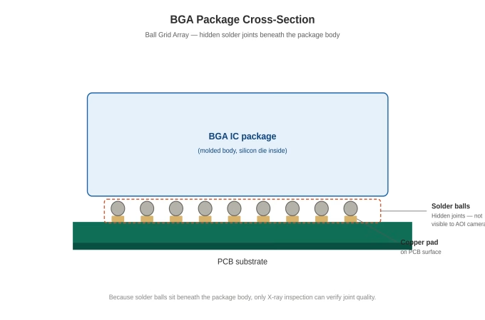
Figure 1 — BGA package cross-section showing the solder ball grid array and hidden joint locations beneath the component
Quad Flat No-lead (QFN)
QFN packages are small, leadless components designed for surface mounting, with exposed copper pads on the underside that solder directly to the PCB. QFNs are valued for their low profile, strong thermal performance (thanks to a large central thermal pad), and compact size. As with BGA devices, QFN solder joints are mostly hidden beneath the package, making visual inspection unreliable. Typical QFN soldering defects include voids under the thermal pad, bridging between adjacent pads, and insufficient solder volume leading to open circuits.
Both BGA and QFN devices are cornerstones of modern miniaturized electronics — from smartphones and wearables to automotive electronics and medical devices — which is why robust BGA and QFN PCB assembly and inspection protocols are non-negotiable for any PCBA manufacturer.
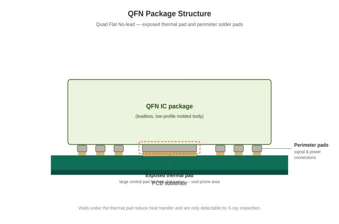
Figure 2 — QFN package structure highlighting the exposed thermal pad and perimeter solder pads
3. Key Assembly Technologies for High-Density PCBs
Achieving high-yield assembly for BGA and QFN devices requires precision at every stage of the surface mount technology (SMT) process. Here are the critical technologies involved in modern high-density PCB assembly.
3.1 Solder Paste Printing
The foundation of a good solder joint is accurate solder paste deposition. For high-density, fine-pitch components, stencil printing technology must be highly precise.
- High-Precision Stencils: Stencils made with laser-cut or electroformed technologies ensure accurate aperture shapes and sizes, crucial for fine-pitch BGA and QFN pads.
- Solder Paste Inspection (SPI): 3D SPI systems are essential for verifying the volume, height, area, and registration of solder paste deposits immediately after printing. Solder paste inspection for BGA and QFN pads can detect insufficient or excessive paste — a major root cause of opens, shorts, and voids — and feed real-time data back into process control.
- Automated Paste Dispensing: For very specific or challenging applications, automated solder paste dispensing can complement or even replace stencil printing, offering unparalleled flexibility and precision for individual pads.
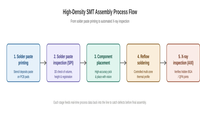
Figure 3 — SMT assembly process flow for high-density PCBA — from solder paste printing and pick-and-place to reflow soldering
3.2 Component Placement (Pick & Place)
Accurate placement of BGA and QFN devices is critical to ensure proper alignment of solder balls or pads with their respective PCB pads.
- High-Accuracy Pick & Place Machines: Modern SMT pick-and-place machines feature high-resolution vision systems, precision motion control, and advanced algorithms to place components with sub-micron accuracy. Fiducial recognition on both the PCB and component is vital.
- Force Control: Some machines offer precise force control during placement, preventing damage to delicate components or excessive pressure that could squash solder paste.
- Package Recognition: Advanced vision systems can identify package types and orientations, correcting for minor misalignments before placement.
3.3 Reflow Soldering
The reflow process melts the solder paste to form the electrical and mechanical connections. A precisely controlled thermal profile is crucial for reliable BGA and QFN solder joints.
- Multi-Zone Reflow Ovens: Ovens with multiple independent heating zones allow for highly precise thermal profiling, crucial for achieving the correct ramp rates, soak times, peak temperatures, and cooling rates.
- Nitrogen Atmosphere: Using a nitrogen atmosphere during reflow can minimize oxidation, improve solder wetting, and reduce solder voids — especially beneficial for fine-pitch and thermally sensitive components.
- Thermal Profiling: Regular profiling of the reflow oven with thermocouples attached to test PCBs ensures the process remains within specification, helping prevent excessive voiding, cold joints, or thermal damage to components.
Here’s a comparison of common BGA and QFN solder defects and their root causes:
| Defect Type | Description | Primary Cause(s) | Impact |
| Solder Voids | Gas bubbles trapped within the solder joint. | Insufficient flux activity, poor thermal profile, excessive paste volume, absorbed moisture. | Reduced mechanical strength, increased electrical resistance, poor thermal dissipation. |
| Solder Bridging | Unintended electrical connection between two adjacent pads. | Excessive solder paste, misaligned stencil, component misalignment, paste slump, incorrect reflow profile. | Electrical shorts, device malfunction. |
| Open Circuits | No electrical connection between component and PCB pad. | Insufficient solder paste, component misalignment, non-wetting, lifting during reflow. | Circuit discontinuity, device failure. |
| Head-in-Pillow (BGA) | Solder ball partially or completely disconnects from the solder paste deposit during reflow. | Paste oxidation, coplanarity issues, insufficient paste volume, warpage. | Intermittent connection, electrical failure. |
| Non-Wetting | Solder fails to adhere to component leads or PCB pads. | Contamination, oxidation, incorrect thermal profile, poor flux activity. | Weak or open connections. |
Table 1: Common BGA and QFN Solder Joint Defects and Root Causes
4. The Indispensable Role of X-Ray Inspection
Given that the critical solder joints of BGA and QFN devices are hidden, traditional Automated Optical Inspection (AOI) cannot provide a complete assessment of quality. This is where X-ray inspection for PCB assembly becomes absolutely essential. X-ray technology allows manufacturers to “see through” components and the PCB to analyze the internal structure of solder joints without damaging the assembly — true non-destructive testing.
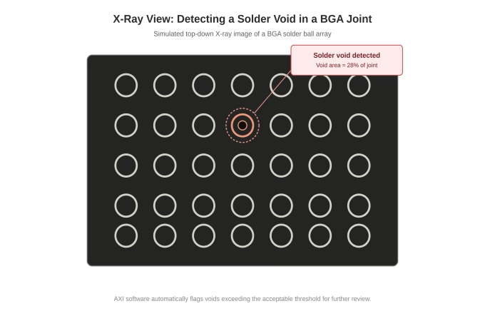
Figure 4 — X-ray image revealing internal solder voids inside a BGA joint that are invisible to standard AOI
Why X-Ray Inspection Is Critical for BGA and QFN PCBA
- Hidden Joint Inspection: Directly inspects solder joints under BGA, QFN, and other hidden-joint packages, including package-on-package (PoP).
- Defect Detection: Identifies critical defects such as solder voids, bridging, open circuits, insufficient or excessive solder, misalignments, and incorrect component polarity — all invisible to AOI.
- Process Control & Optimization: Provides valuable data for process monitoring and fine-tuning. For example, quantifying void percentages in thermal pads helps optimize the reflow profile or stencil design.
- Rework Verification: After rework, X-ray inspectionis crucial to verify the integrity of the repaired joints.
- Failure Analysis: In cases of product failure, X-ray analysis is often the first step in diagnosing the root cause.
5. Advanced X-Ray Inspection Techniques
X-ray inspection systems have evolved significantly, offering various levels of capability to meet different high-density PCBA manufacturing demands.
5.1 2D X-Ray Inspection (2D-AXI)
Basic 2D X-ray inspection provides a two-dimensional image of the solder joints. It is excellent for detecting voids, bridging, and misalignments. Operators can manipulate the board and X-ray source to view joints from different angles, enhancing defect detection.
- Benefits: Relatively fast, good for common defects, provides immediate visual feedback.
- Limitations: Can suffer from image superposition, where features on different layers overlap — making it challenging to differentiate defects in complex assemblies or PoP packages. Requires skilled operators for interpretation.
5.2 3D X-Ray Inspection (3D-AXI)
True 3D X-ray systems, often using computed tomography (CT) or laminography, reconstruct a three-dimensional model of the solder joints. This eliminates the problem of superposition and provides a much more comprehensive view of the joint structure — making 3D AXI for BGA voids the gold standard for complex boards.
- Benefits: Eliminates superposition, provides volumetric analysis of voids, allows cross-sectional views, and is ideal for PoP and very dense boards.
- Limitations: Slower inspection times compared with 2D, higher equipment cost, larger data files.
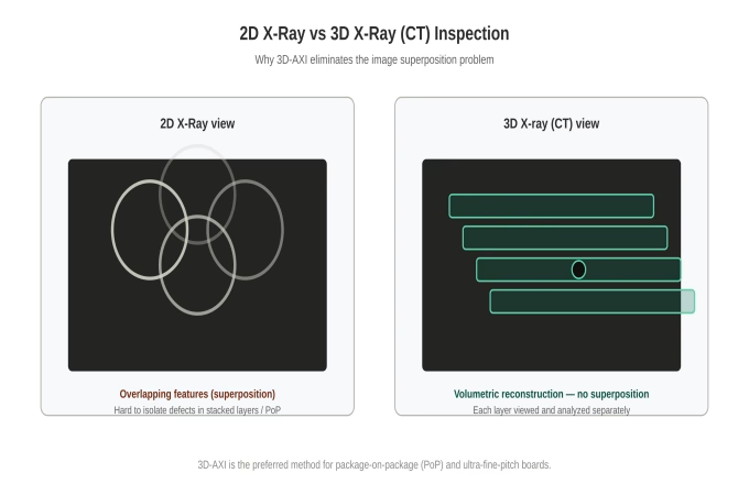
Figure 5 — Side-by-side comparison of 2D X-ray imaging versus 3D X-ray/CT reconstruction of a BGA solder joint
5.3 Automated X-Ray Inspection (AXI)
AXI systems combine X-ray imaging with powerful software algorithms to automatically detect and classify defects without human intervention. This significantly increases inspection speed, consistency, and accuracy, making it suitable for high-volume production lines.
- Offline AXI: Used for sampling or detailed analysis of specific boards.
- Inline AXI: Integrated directly into the SMT line, providing real-time feedback and allowing 100% inspection of boards — crucial for preventing defective products from moving further down the line.
Modern AXI systems often incorporate advanced features such as:
- AI and Machine Learning: Used to improve defect recognition, reduce false calls, and adapt to new component types.
- Advanced Image Processing: Techniques to enhance contrast, reduce noise, and highlight subtle defects.
- Statistical Process Control (SPC): Integration with factory management systems to track defect trends and proactively address process deviations.
| Inspection Type | Key Capability | Best Use Case | Main Limitation |
| 2D-AXI | Fast two-dimensional imaging of solder joints from multiple angles. | Routine inspection of standard BGA/QFN joints. | Image superposition on complex or PoP boards. |
| 3D-AXI (CT / Laminography) | Volumetric 3D reconstruction that eliminates superposition. | Package-on-package (PoP) and ultra-fine-pitch boards. | Slower throughput, higher equipment cost. |
| Automated X-Ray Inspection (AXI) | AI-assisted automatic defect detection and classification. | High-volume lines requiring 100% inspection. | Requires algorithm tuning to minimize false calls. |
Table 2: Comparing 2D-AXI, 3D-AXI, and Automated X-Ray Inspection (AXI)
6. Best Practices and Future Outlook
To maximize yields and ensure reliability when assembling high-density BGA and QFN devices, manufacturers should adhere to several best practices for PCB assembly and inspection:
- Design for Manufacturability (DfM): Collaborate early with design teams to ensure PCB layout and component selection are optimized for assembly and inspection.
- Material Selection: Use high-quality solder paste and flux suitable for the specific package types and reflow profiles.
- Process Control: Implement rigorous control over solder paste printing, component placement, and reflow profiles. Use SPI and AXI data for continuous process improvement.
- Maintenance: Regular calibration and maintenance of all SMT and inspection equipment are critical for consistent performance.
- Operator Training: Ensure technicians and operators are highly trained in both assembly processes and X-ray image interpretation.
- Data Integration: Integrate data from SPI, AOI, and AXI systems for a holistic view of the production process and early detection of trends.
| Best Practice Area | Recommended Action |
| Design for Manufacturability | Engage design teams early to optimize pad layout and component placement for assembly and inspection. |
| Material Selection | Validate solder paste and flux for the specific package type and reflow profile before mass production. |
| Process Control | Use closed-loop SPI and AXI data to continuously fine-tune printing, placement, and reflow parameters. |
| Equipment Maintenance | Calibrate SMT and X-ray inspection equipment on a fixed, documented schedule. |
| Operator Training | Train technicians in both SMT assembly workflows and X-ray image interpretation. |
| Data Integration | Combine SPI, AOI, and AXI data for end-to-end traceability and root-cause analysis. |
Table 3: Best Practice Checklist for High-Density PCB Assembly
The future of high-density PCB assembly and inspection will likely see even greater integration of AI-driven PCBA inspection, predictive maintenance, and further advancements in 3D X-ray technology for even finer-pitch components and more complex PoP structures. Miniaturization continues unabated, driving the need for increasingly sophisticated tools to ensure quality and reliability in the next generation of electronics.
7. FAQ
Question 1: What is the main limitation of AOI for BGA and QFN devices?
Answer: The main limitation is that AOI (Automated Optical Inspection) is primarily a visual inspection method. Since the critical solder joints of BGA and QFN devices are hidden underneath the component body, AOI cannot directly inspect these connections for defects like voids, shorts, or open circuits.
Question 2: Can 2D X-ray inspection replace 3D X-ray?
Answer: Not entirely. While 2D X-ray is effective for many defects, its major limitation is image superposition, especially on complex, multi-layered boards or package-on-package (PoP) assemblies. 3D X-ray (CT or laminography) eliminates superposition by creating a volumetric reconstruction, offering a more complete and unambiguous view of the solder joints. The right choice depends on the specific complexity and inspection requirements of the board.
Question 3: How important is the thermal profile in reflow soldering for BGA/QFN?
Answer: The thermal profile is extremely important. An incorrect profile can lead to numerous defects such as excessive voiding, insufficient wetting, cold joints, bridging, and even component damage. A precisely controlled profile ensures optimal solder melting, wetting, and solidification — crucial for robust and reliable connections, particularly given sensitive BGA and QFN thermal characteristics.
Question 4: What is the benefit of using nitrogen in the reflow oven?
Answer: Using a nitrogen atmosphere in the reflow oven reduces oxidation of solder paste and component pads. This improves solder wettability, reduces surface tension, and can significantly decrease the formation of solder voids, leading to stronger, more reliable, and cosmetically superior solder joints — especially beneficial for fine-pitch and thermally sensitive components.
Question 5: What causes solder voids in BGA packages?
Answer: BGA solder voids typically form from trapped gas during reflow, caused by insufficient flux activity, an incorrect thermal profile, excessive paste volume, or moisture absorbed by the paste before printing. Controlling these variables and verifying results with X-ray inspection keeps void levels within acceptable limits.
Question 6: How do I choose between inline and offline AXI for PCBA production?
Answer: Inline AXI is best suited for high-volume lines that need 100% X-ray inspection and real-time defect feedback, while offline AXI is more practical for sampling, engineering analysis, or lower-volume runs where a dedicated inline system isn’t cost-justified.
8. Summary
The assembly of high-density BGA and QFN devices is a cornerstone of modern electronics manufacturing, enabling the creation of compact, high-performance products. However, the intricate nature of these components presents significant challenges, particularly in ensuring the integrity of hidden solder joints. Mastering this process requires a sophisticated combination of advanced SMT technologies, including high-precision solder paste printing with SPI, accurate component placement using cutting-edge pick-and-place machines, and tightly controlled reflow soldering with optimized thermal profiles.
Crucially, X-ray inspection stands as an indispensable tool in this ecosystem, providing the ability to non-destructively examine hidden solder joints for critical defects that are invisible to optical methods. Whether through 2D, 3D, or fully automated AXI systems, X-ray inspection for PCB assembly ensures quality control, facilitates process optimization, and underpins the reliability of complex electronic assemblies. By integrating these key technologies and adhering to best practices, manufacturers can overcome the challenges of high-density BGA and QFN PCB assembly and continue to push the boundaries of electronic innovation.
9. Key Takeaways
- High-density BGA and QFN devices are critical for miniaturization but pose significant assembly and inspection challenges due to hidden solder joints.
- Precision in solder paste printing (enabled by SPI), component placement, and reflow soldering with controlled thermal profiles is foundational for high-yield assembly.
- X-ray inspection is non-negotiable for BGA and QFN devices, as it allows detection of hidden defects like voids, shorts, and opens.
- Advanced X-ray techniques — including 2D-AXI, 3D-AXI, and fully Automated X-ray Inspection — offer varying levels of detail and automation for defect detection and process control.
- Integrating DfM, robust process control, continuous data analysis, and highly trained personnel are essential best practices for success in high-density PCB manufacturing.
Contact Us
Phone: +86-18123905375
Email: sales@assemblepcb.com
WhatsApp: +86-18123905375
Wechat: +86-18123905375
Free Queto
Latest Blog

Table Of Contents
Contact Us
Phone: +86-18123905375
Email: sales@assemblepcb.com
WhatsApp: +86-18123905375
Wechat: +86-18123905375
Free Queto
