
SMD Components: Types, Sizes, Codes and Identification
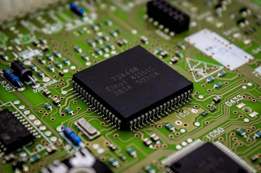
Table Of Contents
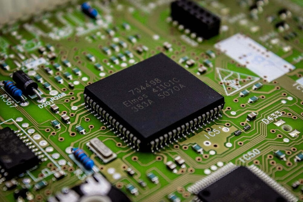
SMD components are electronic parts designed to be soldered onto pads on the surface of a printed circuit board. They include resistors, capacitors, inductors, diodes, transistors and integrated circuits. Their small footprints support compact assemblies, but selecting or identifying them requires more than recognizing a package shape.
This guide explains the main component families, common package sizes, value markings and practical selection checks. Start with the approved BOM and manufacturer datasheet whenever they are available: a body code or photograph alone rarely establishes a complete part specification.
1. Understanding SMD Components
A surface-mount device connects to PCB surface pads through terminals, leads or solder balls. Through-hole parts instead use leads inserted into board holes. Both technologies can appear on the same board; a connector or mechanically loaded part may still use through-hole mounting.
SMD vs SMT: component and assembly process
SMD means surface-mount device; SMT means surface-mount technology, the process used to place and solder those devices. A resistor is an SMD component, while stencil printing, placement and reflow are SMT process steps.
Smaller parts and mounting on both sides can increase circuit density. However, the smallest available package is not automatically the best choice. Power dissipation, inspection access, handling, repair and assembly capability also matter. Automated placement can improve repeatability, but it does not remove the need for a verified footprint, orientation and process setup.
2. Basic Types of SMD Components
| Family | Typical circuit role | Checks beyond the nominal value |
|---|---|---|
| Resistor | Current limiting, biasing, feedback or sensing | Tolerance, power, working voltage, pulse rating and temperature coefficient |
| Capacitor | Decoupling, filtering and energy storage | Voltage, dielectric, effective capacitance, ESR, ripple and polarity |
| Inductor / ferrite bead | Energy storage, filtering or noise suppression | Current limits, DCR, frequency behavior and the intended function |
| Diode / LED | Rectification, clamping, switching or light emission | Polarity, current, reverse voltage, losses and thermal limits |
| Transistor | Switching or amplification | Pinout, drive requirements, voltage, current and thermal performance |
| Integrated circuit | Processing, control, conversion or communication | Exact ordering code, pinout, supply, package and firmware requirements |
2.1 Resistors
Chip resistors set currents and voltages or provide feedback and signal termination. Thick-film devices are common in general-purpose circuits. Thin-film and other precision technologies serve applications that need tighter tolerance, low drift or specified noise performance. These categories do not have one universal resistance range.
For a current-sense resistor, calculate the voltage drop and heating at the intended current, then check pulse behavior and the recommended sensing layout. For any resistor, verify the manufacturer’s derating conditions rather than assigning a power rating solely from its body size. Our resistor sourcing and assembly page covers the procurement side of an approved BOM.
2.2 Capacitors
Multilayer ceramic capacitors (MLCCs) are widely used for decoupling and filtering. They are normally nonpolarized, but dielectric selection matters: a nominal capacitance value does not describe performance under every operating condition.
High-permittivity ceramics such as X5R and X7R can lose effective capacitance under DC bias. C0G parts have different stability characteristics and are useful where capacitance stability matters. Compare the actual part curves, not just the capacitance and rated voltage printed in a catalog. Murata explains this DC-bias effect.
Tantalum, aluminum electrolytic, polymer and film capacitors offer different trade-offs in capacitance, ESR, leakage, frequency behavior and lifetime. Many tantalum and electrolytic devices are polarized. Check the datasheet’s polarity convention, ripple limits and application guidance; one capacitor technology is not universally superior to another.
2.3 Inductors
Inductors store energy in a magnetic field and appear in power converters, RF networks and filters. Construction may be wirewound, multilayer or another form suited to the application. A ferrite bead is chosen primarily for its impedance over a noise-frequency range; it should not be substituted for an energy-storage inductor merely because the package fits.
For power inductors, distinguish saturation current from RMS current: one concerns loss of inductance under bias and the other a specified temperature rise. Also check DCR, operating temperature and frequency-dependent losses. Coilcraft’s current and temperature guidance explains why these limits must be interpreted together.
3. Semiconductor SMD Component Types
3.1 Diodes
Rectifier, Schottky, Zener, TVS and LED devices perform different jobs. Select a diode by its function, forward current, reverse-voltage requirement, switching behavior and thermal conditions. A Zener can provide an approximate voltage reference over its specified operating-current range; it does not maintain a constant current by itself.
A stripe often indicates the cathode on a discrete diode, but package conventions must be verified. LED polarity marks also vary. Use the manufacturer’s package drawing and the PCB assembly drawing together, especially when the silkscreen mark is ambiguous.
3.2 Transistors
A single bipolar junction transistor (BJT) has three electrical terminals: base, collector and emitter. NPN and PNP types have different bias polarities. Their pin order is not determined by an SOT-23 outline alone. Nexperia’s BJT handbook provides manufacturer guidance on device behavior and circuit configurations.
MOSFETs use gate, drain and source terminals. Enhancement-mode devices are normally off at zero gate-to-source voltage; depletion-mode devices are normally on. Do not use threshold voltage as proof that a MOSFET is fully enhanced at the available gate drive: check the specified on-resistance and operating conditions. See Infineon’s MOSFET explanation for the operating-mode distinction.
The package may contain a single transistor, a pair or additional circuitry. Verify the full part number and pin assignment before selecting a replacement.
3.3 Integrated Circuits
Surface-mount ICs include microcontrollers, memory, amplifiers, converters, interface devices and power-management circuits. Common outlines include SOIC, TSSOP, QFP, QFN and BGA. An outline describes packaging, not the device’s function.
Match the complete ordering code, package dimensions, pin count, pitch and pin-one orientation. Exposed pads may require a specific electrical connection and thermal layout. BGA connections sit underneath the package, so inspection and rework requirements differ from those for accessible leads. For those assembly details, use our BGA and QFN assembly inspection guide.
4. SMD Component Sizes, Codes and Identification
Keep package codes, value codes and part numbers separate. A code such as 0603 usually describes a chip body size under a stated unit system. A resistor marking such as 103 describes a resistance value under a particular marking scheme. Neither supplies the complete electrical specification.
The table below gives common nominal dimensions for rectangular chip passives. These are body dimensions, not PCB land-pattern dimensions. Actual dimensions and tolerances depend on the series; use its package and recommended land-pattern drawings.
| Imperial designation | Common metric designation | Nominal length × width |
|---|---|---|
| 0201 | 0603 | 0.6 × 0.3 mm |
| 0402 | 1005 | 1.0 × 0.5 mm |
| 0603 | 1608 | 1.6 × 0.8 mm |
| 0805 | 2012 | 2.0 × 1.25 mm |
| 1206 | 3216 | 3.2 × 1.6 mm |
| 1210 | 3225 | 3.2 × 2.5 mm |
0603 is ambiguous without the unit system: imperial 0603 is approximately 1.6 × 0.8 mm, while metric 0603 is approximately 0.6 × 0.3 mm. Explicitly state the system in drawings and purchasing data. Murata’s product catalog illustrates nominal chip dimensions alongside inch-based size designations; consult current part-specific data for a new design.
4.1 Resistor Sizes and SMD Resistor Codes
In a common three-digit resistor marking, the first two digits are significant figures and the last digit is a power-of-ten multiplier in ohms. A four-digit marking uses three significant figures followed by the multiplier. R can act as a decimal point. These conventions are illustrated in Vishay’s resistor coding reference.
| Marking | Interpretation under the stated scheme | Value |
|---|---|---|
| 103 | 10 × 10³ Ω, three-digit scheme | 10 kΩ |
| 1002 | 100 × 10² Ω, four-digit scheme | 10 kΩ |
| 4R7 | R is the decimal point | 4.7 Ω |
EIA-96 markings use a lookup system rather than the same digit rule. Very small resistors may be unmarked. Obtain tolerance, power and voltage limits from the exact datasheet and reel label; the value marking alone does not establish them.
4.2 Capacitor Sizes and SMD Capacitor Codes
Many small MLCCs have no readable body marking. Their appearance cannot reliably reveal capacitance, voltage rating or dielectric. Keep the reel label and BOM association intact, or use the board documentation to identify a fitted part.
Where a capacitor manufacturer uses the familiar three-digit capacitance scheme, 104 means 10 × 10⁴ pF = 100 nF = 0.1 µF. This code does not itself state the voltage rating. SMD capacitor codes on molded tantalum or electrolytic parts can follow other conventions; consult the series marking diagram instead of applying the MLCC example to every capacitor.
4.3 Inductor Sizes and Codes
Inductor markings vary by manufacturer and series, and some parts are unmarked. Do not assume every inductor uses a four-digit code or the same units. A body size and inductance value also do not establish saturation current, DCR or RF suitability.
4.4 A Practical SMD Component Identification Workflow
- Disconnect power and discharge stored energy before examining the board. Record its revision and the component reference designator.
- Compare the schematic, BOM and assembly drawing. A designator such as R, C, L, D, Q or U is a useful clue, but board naming conventions vary.
- Photograph all markings and orientation features under magnification. Measure the body and count the terminals; do not confuse a date or lot code with a part number.
- Use the suspected manufacturer’s marking resources, then compare the datasheet package, pinout and circuit role. For TI parts, the official part-marking lookup is one starting point.
- If needed, make appropriate unpowered measurements. Parallel circuit paths can affect in-circuit readings, and a meter cannot recover an unknown voltage rating. Record uncertainty rather than approving a substitute from a short code alone.
5. Selection and Application of SMD Components
5.1 Electrical Characteristics
Specify the required value and tolerance, then check operating voltage, current, temperature, frequency and transients. Distinguish recommended operating conditions from absolute maximum ratings. For passives, review behavior under actual bias and load; for semiconductors, check supply compatibility and input/output limits.
5.2 Physical Dimensions
Verify body dimensions, height, terminal geometry, pitch and the recommended land pattern. Two parts with similar body sizes may need different footprints. Check stencil, placement, inspection and rework capability with the assembler before shrinking the design.
5.3 Compatibility with Other Components
Review pin mapping, polarity, thermal paths and interactions with the surrounding circuit. A capacitor substitution may change regulator stability through its ESR or effective capacitance. A different transistor may need different drive conditions. Approve alternatives by electrical, mechanical and process requirements, not by nominal value alone.
5.4 Examples of SMD Component Selection and Application
- Microcontroller decoupling: start with the IC manufacturer’s recommendations, check effective capacitance at the supply voltage and place the parts with an appropriate return path.
- DC-DC converter: verify inductor saturation and thermal limits against peak and RMS current, and check capacitor ripple performance and control-loop requirements.
- Precision measurement: review resistor ratio accuracy, temperature drift and self-heating instead of selecting solely by initial tolerance.
For a build review, provide manufacturer part numbers, quantities, package details, approved alternatives and any do-not-populate positions. Our PCB assembly service can be included in the same project enquiry; the actual component and process requirements should be agreed for that build.
6. Soldering SMD Components
6.1 Soldering Techniques
A common SMT flow applies solder paste through a stencil or a controlled dispensing process, places components, then reflows the assembly. Pick-and-place equipment normally positions the components; it should not be described as the general solder-paste printing step.
Verify paste condition, aperture design, orientation and the measured board profile. Use component and solder-material limits to define heating and cooling. Hidden BGA or QFN interfaces require suitable inspection; a visually tidy exterior does not prove that every joint underneath is acceptable.
Manual work may suit accessible terminals when the component allows it. Use an appropriate tip or nozzle, flux and controlled heating, and avoid pulling a component while solder is still solid. Inspect for bridges, lifted pads and nearby damage, then carry out the required electrical checks. For diagnosing a weak connection, see the separate cold solder joint repair guide.
6.2 Handling Precautions
Use an ESD-controlled workstation and suitable tools for sensitive devices. Keep part identification with the packaging and avoid excessive board flex or force on ceramic components. Observe moisture-sensitivity labels, floor life and the manufacturer’s storage or baking instructions; baking is not a universal remedy for every part. TI’s quality and packaging FAQs explain moisture-sensitive handling.
There is no universal 350–380°C removal setting. A tool setpoint is not the component-body or solder-joint temperature. Follow a qualified rework process for the board, alloy and device, and respect time and thermal limits. Murata’s MLCC rework guidance addresses thermal-shock and handling concerns.
7. Summary
Choose SMD components by circuit function, verified electrical limits, package compatibility and assembly requirements. Keep size designations separate from value markings, and treat uncertain identification as a reason to check documentation. A correct BOM and footprint prevent mistakes that a short body code cannot resolve.
Preparing a build? Send your BOM, assembly drawings and build quantities for a project-specific review. Include critical ratings, approved substitutes and inspection requirements so the enquiry can address the actual design.
8. FAQs
What are SMD components?
They are surface-mount devices designed to connect directly to PCB surface pads. Common examples include chip resistors, MLCCs, diodes, transistors and ICs.
What is the difference between SMD and SMT?
SMD describes the device; SMT describes the mounting and soldering technology. Both terms may appear in an assembly discussion, but they refer to different things.
How do I identify an unmarked SMD component?
Start with the BOM, schematic and reference designator. Add package measurements and circuit context, then verify the manufacturer data. Appearance or an in-circuit meter reading alone cannot establish every rating or identify every unmarked component.
Are 0603 and 1608 the same size?
Imperial 0603 and metric 1608 commonly describe a nominal 1.6 × 0.8 mm chip. Metric 0603 is much smaller. State the unit system and check the exact package drawing.
Does a 103 marking mean the same thing on every component?
No. Under a common resistor marking scheme it means 10 kΩ. Other component families and manufacturers can use different conventions. Identify the part family and marking system first.
Can I replace an SMD part with any part of the same size?
No. Match function, pinout, ratings, operating behavior, footprint and assembly requirements. Record and approve the substitute before production.
Contact Us
Phone: +86-18123905375
Email: sales@assemblepcb.com
WhatsApp: +86-18123905375
Wechat: +86-18123905375
Free Queto
Latest Blog


Table Of Contents
Contact Us
Phone: +86-18123905375
Email: sales@assemblepcb.com
WhatsApp: +86-18123905375
Wechat: +86-18123905375
Free Queto
