
Flying Probe Testing for Low-Volume PCB Assembly: Coverage, Files, and When to Use ICT
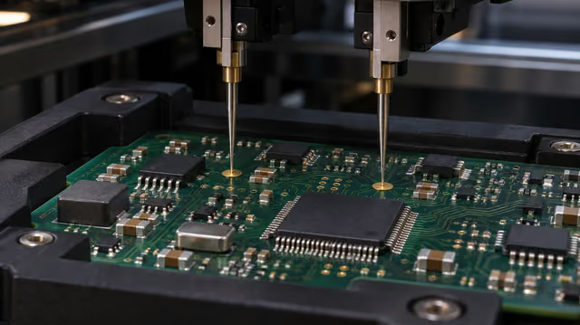
Table Of Contents
Generated illustration of an assembled board in a flying probe station.
Use flying probe testing for prototypes and small PCB assembly runs when the accessible nodes support the checks you need and the design may still change. Ask your supplier for a coverage list before approving the quote. Revisit fixture-based in-circuit testing (ICT) when the board revision stabilizes and the savings on repeat units can pay for tooling and validation.
At AssemblePCB, we review low-volume builds for manufacturing and assembly constraints and scope functional testing around the project requirements. If you need flying probe testing, send us the board revision, expected build quantities, and the faults you need to catch. That gives us a starting point for reviewing test access and quoting the work.
What Flying Probe Testing Covers on an Assembled PCB
A flying probe tester moves programmable probes to accessible pads, vias, or leads and takes electrical measurements defined in a test program. A standard carrier or edge clamps support the board. The test engineer programs the sequence, verifies reliable contact, and sets limits for the actual assembly. The measurement options vary by machine and by circuit.
Bare-board continuity vs. assembled-board checks
Bare-board electrical test checks the fabricated board for opens and shorts against the expected connectivity. After population, components create electrical paths of their own. On an assembled board, the test engineer has to account for those paths before deciding what constitutes an open, a short, or an out-of-tolerance component reading. Ask for both steps explicitly when your purchase order covers fabrication and assembly.
| Failure mode or requirement | Possible flying probe check | What to verify before release |
|---|---|---|
| Open on a critical connection | Continuity between accessible locations that bracket the path | Confirm the actual joint lies in the measurement path and a parallel path cannot mask the open. |
| Short or solder bridge | Check isolation between selected nets, such as a rail and ground, using suitable limits | Account for charging capacitors and intentional low-resistance paths. |
| Wrong passive value | Measure resistance or capacitance where access and circuit topology permit | Review parallel components and tolerances. Some values can only be inferred or may lack direct coverage. |
| Hidden BGA or QFN joint | Electrical evidence may catch a fault when accessible nodes expose the affected path | Use a suitable X-ray inspection plan when joint geometry or voiding is part of the acceptance criteria. |
| Firmware boot or interface behavior | Some systems can support specified powered checks with the right setup | Use a defined functional test for required boot, communications, I/O, or load behavior. |
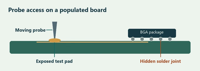
Ask for a list of covered and uncovered faults. If a report quotes a coverage percentage, confirm its denominator. A percentage of accessible nets answers a different question from a percentage of component faults. If a standard supplier report gives net access only, add a short list of product-critical faults and how each will be checked.
Confirm what the proposed tester can reach and measure
Flying probe coverage depends on the proposed machine, the populated board, and the programmed checks. Ask whether the setup can probe the required side or both sides, what clearance it needs around tall parts, and how the board will be supported. If a powered check is required, confirm how power is applied and which signals the system can stimulate or measure. Ask for confirmation on your board revision and panel rather than relying on a machine’s nominal minimum pad size.
Flying Probe Test Files to Send With an RFQ
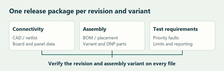
Send one release package for each PCB revision and assembly variant. Confirm the import format with the test provider before exporting. A structured CAD export such as ODB++ or IPC-2581 may work if the supplier supports it. A Gerber-based release generally needs companion files to supply connectivity and component information.
- Board geometry and connectivity. Supply the agreed CAD dataset or Gerber and NC drill data with the requested layout netlist, such as IPC-D-356/356A where applicable. Include board outline, side conventions, and panel-to-board coordinates when using a panel.
- Assembly definition. Include the schematic, BOM, pick-and-place data, and assembly drawing. Identify do-not-populate (DNP) parts, approved alternates that affect limits, polarity, and the exact variant being quoted.
- Test intent and reporting. Mark priority nets and accessible points. Specify test side, keep-outs, approved powered conditions if applicable, limits, and any reporting or serial-number traceability requirements.
- Validation material. Ask how many samples the supplier needs, whether a verified reference assembly is helpful, and how the program will be validated against faults. A known-good board can help verify expected readings, while a safely simulated fault can show whether a critical test detects its intended failure.
Check access with the board populated
A point that looks reachable in the layout can sit beneath a shield, beside a tall connector, under solder mask, or inside a clamp zone. Ask the supplier to check access on the populated board and confirm the panel orientation and coordinate origin. If a critical point is blocked, decide whether to test before fitting the obstructing part, add access in the next revision, or cover the fault with another method.
Worked example of a test pad blocked by a shield
Consider a dense controller board with a soldered RF shield. The layout shows a pad on the regulator-enable net under the shield. A pre-shield check can verify a specified path at that stage. It leaves the supplier to decide how to check for faults introduced during shield installation.
For the current revision, look for an exposed point on the same net and verify that the probe pair still brackets the connection of interest. If final electrical access is unavailable, document the coverage gap and agree on a powered enable check if that check detects the failure you care about. On the next revision, place an accessible test pad outside the shield and the clamp area. Record which check covers pre-shield assembly and which check applies to the finished board.
How to Tell Poor Probe Contact From a Real Open
A repeat open at the same coordinate can come from the board, the test program, or the probe contact. Preserve the first failure and use a controlled check before deciding how to disposition the unit.
- Check the landing point. Confirm the board side, panel position, origin, and coordinates against the released files. Inspect the pad for mask encroachment, residue, damage, or a probe mark off the pad. Confirm the clamp holds the board flat and the tip is clean and undamaged.
- Compare a verified reference board. Use the same program and setup. If the same point fails on a verified good board too, investigate the setup or program before treating the original result as an assembly defect.
- Verify the intended path through independent access. When approved, check the suspect connection using other pads that still bracket the joint, or use an independent bench measurement. A consistent failure there supports an actual open. Record the original result, what changed, and the final disposition.
If a reading changes after reseating, inspect the board as well as the setup. Both contact issues and intermittent joints can produce changing readings. Keep the unit under review until the agreed retest procedure resolves the failure.
Flying Probe Testing vs. ICT: When the Fixture Pays Off
Fixture-based ICT becomes a cost candidate when expected savings per board cover the extra upfront investment. Flying probe usually has lower upfront tooling cost. Fixture-based ICT can contact many points in parallel and often reduces cycle time after setup. Compare fixture-compatible volume, required coverage, line capacity, and the cost of changes.
Calculate break-even for the same test scope
Break-even quantity = (ICT fixed cost − flying probe fixed cost) ÷ (flying probe cost per board − ICT cost per board)
Use fixed costs for programming, fixture, validation, and any quoted changeover costs treated as upfront. Use the quoted variable cost per board on both sides. This calculation assumes comparable coverage, constant variable costs over the volumes considered, higher fixed costs for ICT, and lower per-board costs for ICT.
Illustrative example, in USD. A flying probe quote has $350 fixed + $4.20 per board. ICT has $3,250 fixed + $1.30 per board. The difference is $2,900 upfront and $2.90 per unit, so the two quotes meet at 1,000 boards, at $4,550 each. At 300 boards, flying probe costs $1,610 and ICT costs $3,640. At 1,500 boards, the totals are $6,650 and $5,200. These are hypothetical quotes used to show the calculation.
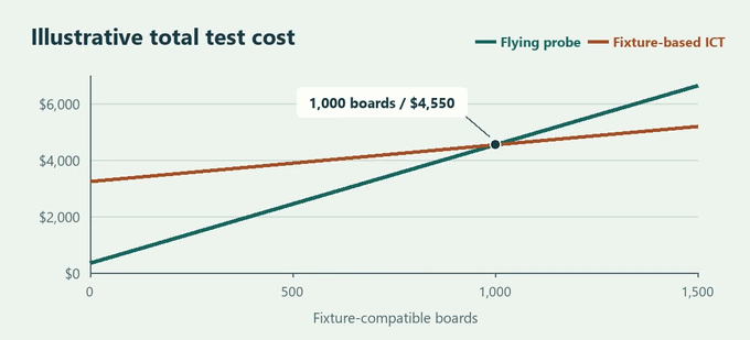
Count the units you expect to build before the next fixture-affecting change. If throughput or customer acceptance requires additional checks, compare complete test plans. Include the differences in engineering time and test cost before making the decision.
Approve the First Run Against the Test Plan
AssemblePCB’s published SMT inspection workflow includes solder paste inspection, automated optical inspection, first-article checks, and X-ray for hidden joints. When you request a quote, identify which faults need an electrical test and which need inspection or a powered functional check. That lets the build team assign a method, acceptance criteria, and reporting requirements to each critical item.
- Agree on coverage before programming. List the critical faults, the released board and variant, and the complementary checks for excluded faults.
- Review the first assemblies and the sample report. Ask how the provider distinguished poor probe contact from a true open and validated critical pass/fail limits.
- Verify traceability before releasing the lot. Confirm how failures are recorded, when retests are permitted, and which revision of the test program goes with the lot. Request serial-number linkage if your project requires it.
If the first run needs hidden-joint inspection, review the BGA and QFN X-ray inspection guide before agreeing on sampling and acceptance criteria.
Frequently Asked Questions
Can flying probe testing work without dedicated test pads?
Sometimes. Exposed vias or component leads can be usable when their geometry, surface, and clearance allow safe, repeatable contact. Ask for a reachability review before committing to a particular coverage target.
Can flying probe testing replace functional testing?
Use a functional test whenever acceptance depends on actual product behavior. A continuity or component reading cannot establish that firmware boots, a communication port exchanges data, or an output operates under its intended load.
Should I switch to ICT after the first repeat order?
Compare quoted costs using the repeat quantity you expect for the same fixture-compatible design. Ask the supplier which anticipated layout changes can be handled by updating the program and which require fixture work.
Technical References
- SPEA on flying probe tester capabilities
- Eurocircuits on bare-board continuity and isolation testing
- Sierra Circuits on flying probe programming and test workflow
- FixturFab on flying probe and fixture-based ICT trade-offs
Request a Flying Probe Coverage Review From AssemblePCB
Send AssemblePCB your revision-matched CAD or layout netlist, BOM, placement data, pilot and repeat quantities, and the faults your test plan must detect.
Ask us to review which checks are feasible, flag access gaps, and quote the agreed test scope. If both flying probe and fixture-based ICT fit your build, request both prices on the same coverage basis with setup and per-board costs shown separately.
Upload Files and Request a Coverage Review
Use the quote form on the low-volume assembly page, or email our sales team about your test requirements.
Contact Us
Phone: +86-18123905375
Email: sales@assemblepcb.com
WhatsApp: +86-18123905375
Wechat: +86-18123905375
Free Queto
Latest Blog

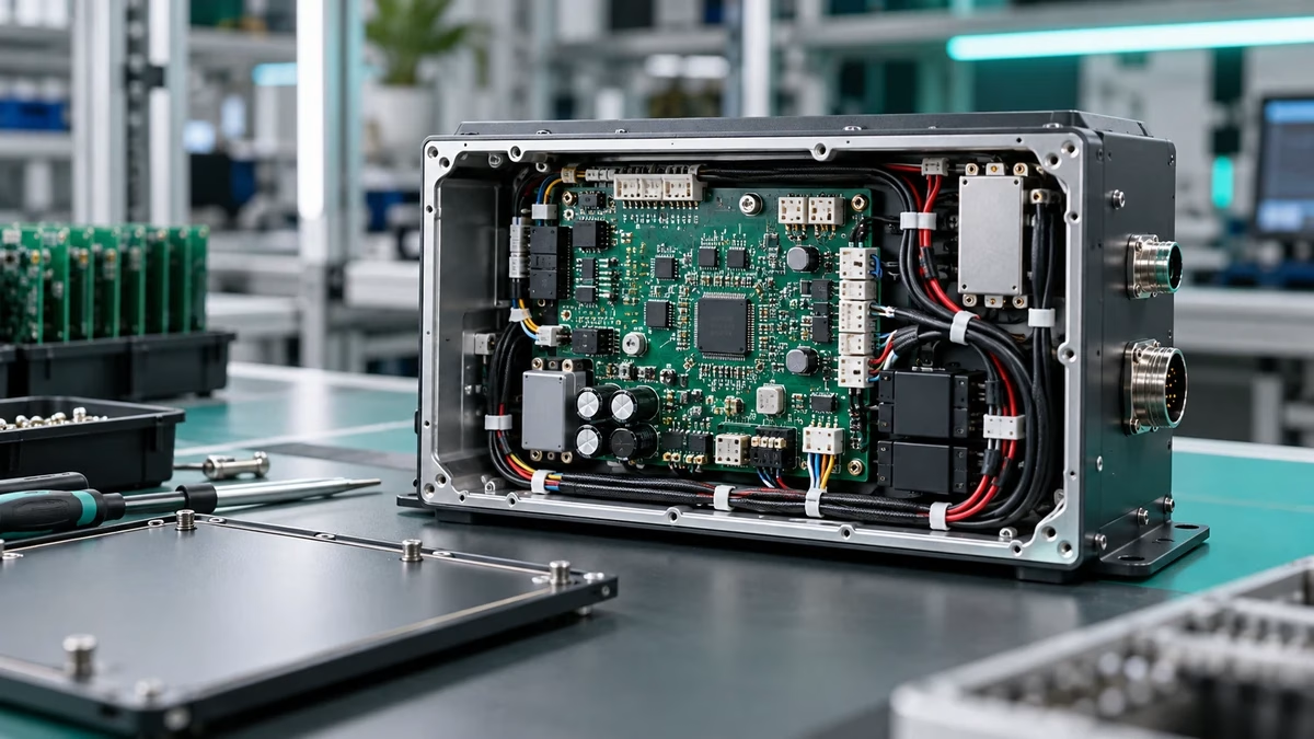

Table Of Contents
Contact Us
Phone: +86-18123905375
Email: sales@assemblepcb.com
WhatsApp: +86-18123905375
Wechat: +86-18123905375
Free Queto
