Typical Issues and Solutions for PCB Assembly
Table Of Contents
Through precise circuit design and component integration, PCBA (Printed Circuit Board Assembly), the “nerve center” of electronic devices, makes signal processing, power distribution, and functional control possible.
Numerous procedural and technical difficulties in its process have an immediate effect on the dependability, quality, and production efficiency of the final product. Common problems and associated technical analysis are listed below.
1.Incoming Material InspectionStage
1.1 Common Issues
1.1.1 Packaging & Component Appearance Defects
Physical damage: Chipped or bent bodies, padsless or bent leads, or cracked packages as a result of improper handling or transport (e.g. QFP/TQFP Pins misaligned or BGA Balls missing).
Corrosion/Oxidation: Surface contamination due to moisture or tarnished lead (e.g. copper oxidation at uncoated terminals).
Labeling errors: Incorrect or missing part numbers, lot code, or polarity markings (e.g. reverse silk-screening on diodes/capacitors), resulting in misidentification of components during assembly.
Packaging Issues: Damaged reels/trays, or improper anti-ESD packing for sensitive devices, e.g. MOSFETs and ICs.
1.1. 2 Dimensional and Specification Mismatches
Footprint discrepancies: Inconsistencies in SMD component dimensions or lead pitches, e.g. SOIC-16 with 1.27mm and 2.54mm spacing, compared to Gerber/BOM files.
Polarity/ Orientation errors: Unmarked polarities, reverse-marked diodes or misaligned Pin 1 indicators on ICs can cause functional failures after soldering.
Material composition issues: Noncompliant substrates, such as FR-4, instead of the specified high-Tg materials for high-temperature application, or incorrect plating, such as tin-lead finishes instead of pure tin.
1.1. 3 Electrical & functional Failures
Deviations in Parameters: Out of tolerance values (e.g. resistors >5% from their rated value or capacitors with ESRs exceeding specs), or unstable performance.
ESD-Induced Damage: Latent defects in electrostatic-sensitive devices (ESD-SD) like CMOS ICs, where internal die cracks or gate oxide breakdown occur during handling but only manifest during functional testing.
Short/Open Circuits: Faulty connectors or multi-lead components with faulty connections (e.g. bridging of IC pins caused by manufacturing defects).
1.1. 4 Environmental Risks
Moisture-Sensitive: Inadequate packaging of MSL 3+ (e.g. QFN, BGA) components, leading to delamination during reflow or “popcorning”.
Poor Solderability: Insufficient tinning of leads (e.g. nickel plating thickness less than 5mm) or contamination (e.g. oil residues on terminals), leading to non-wetting joints or cold joints.
Thermal/Mechanical vulnerabilities: Components that fail to meet the temperature cycling requirements. (e.g. resistors breaking under tests from -40degC up to +85degC) or mechanical stresses (e.g. connectors with an insufficient retention force).
1.1.5 Additional Material Issues
Adhesive failure: Low post-cure bonding strength (5MPa), or Tg below standard.
Cleaning agent residue: Ionic contamination exceeding IPC5701 limits (=1.56mg/cm2 equivalent NaCl).
1.1.6 Documentation and Compliance Gaps
Missing certifications: Absence of RoHS/REACH reports, AEC Q100 automotive qualifications or military grade (MIL-SPEC test data) for specialized applications.
Lot Tracking Issues: Inconsistent codes on components and delivery documents making it difficult to trace back failures to specific manufacturing batches.
Counterfeit parts: Substandard components or fraudulent components, often detected by XRF analysis of material or die photography.
1.1.7 Challenges in Process-Related Issues
Inspection tool limitations: Inadequate Resolution of optical Comparators (failing in detecting 0201-sized component deviances) or miscalibrated BGA solder joints >10%.
Human error: Ignoring subtle defects, such as micro-cracks on ceramic capacitors due to fatigue or misinterpretation in datasheets.
Sampling bias: Inadequate sampling of AQL (Acceptable quality limit) leading to the missed defects in large batch (e.g. testing only 5 pieces from a reel with 5,000 pieces).
1.2 Mitigation Strategies
Standardize Procedures: Use checklists aligned to IPC-A-611/AS9100 (e.g. LCR meters for active components and ICT for passive devices) for visual inspection and automated tests.
Leverage technology: Implement XRF spectrometers to analyze material composition, automated optical inspection for high-volume runs and thermal chambers to screen for reliability.
Supplier collaboration: Implement the PPAP (Production part Approval Process), and conduct regular audits, to ensure traceability. This will reduce the risk of counterfeit parts or non-conforming components.
2.Solder Paste Printing Stage
2.1 Common Issues
2.1.1 Packaging & Component Appearance
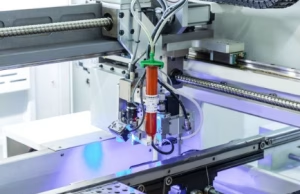
Defects in Solder Paste Deposit :An incorrect stencil design, or excessive wear of the stencil; an uneven squeegee or abnormal angle or pressure; an abnormal paste viscosity; or inadequate agitation when printing can cause localized over/under-deposition. Insufficient thickness can cause cold joints and compromise the mechanical strength of solder joints.
Insufficient Paste/Missing Paste: No paste on pads or partial omission may result from clogged stencil apertures, PCB misalignment, excessive squeegee speed, or inadequate stroke. Manual rework is necessary for open circuits or functional faults brought on by missing solder joints.
Bridging/Excessive paste: Inadequate squeegee pressure, low paste thixotropy or excessive humidity diluting paste, and aperture spacing smaller than IPC-7525 norms might cause paste to join adjacent pads or overlap onto the solder mask.
2.1.2 Alignment and Placement Deviations
Misalignment/Skew of Paste : Faulty positioning of the PCB, inadequate stencil tension and incorrect rail width adjustments can result in partial overlap or displacement. This results in semi-wetted joint prone to cracking when vibration occurs.
Pad Edge contamination: Increased flux residue after soldering can be caused by excessive stencil-PCB gaps and high flux content (>20%).
2.1.3. Paste Quality & Parameter Issues
Paste Oxidation/Drying: Unused or unclean paste that has exceeded its shelf life (>10), long printing breaks without stencil cleaning, and wet sponge covering can result in clogged holes causing missing paste. Oxidized paste can introduce voids of >20% reducing joint strength.
Viscosity anomalies :A deviation from the standard environment or inadequate mixing may result in blurred edges after printing (low viscosity), or paste tails post-printing (high viscosity). Low viscosity can cause collapse/bridging, while high viscosity will reduce paste release. Both of these directly affect soldering yield.
2.1.4 Equipment & Tooling Questions
Stencil damage: Excessive reuse, improper cleaning and nozzle collisions during component placement can result in missing or irregular shapes.
Squeegee wear/Angle Abnormality: Excessive pressure or infrequent blade replacement, as well as mismatched materials, can result in notches/deformations on the squeegees. This results to incomplete solder paste, uneven edges and inconsistent solder joint.
2.2 Mitigation Strategies
Inspection Methods:
Offline SPI for thickness/area/shift (precision +-2mm).
3D AOI to check paste geometry integrity and identify height deviations.
Process control:
Stencil management: nano-coated stencils with reduced residue; post-print ultrasonic cleansing using vacuum suction.
Paste management: FIFO compliance; 4-hour use after opening and =24 hour cold storage of remaining paste.
Standard Compliance:
Acceptance according to IPC-A-611 Class 3: Paste covering >=90% of pad area with a shift 10% in pad width.
3.SMT Component Placement Stage
3.1 Common Issues
3.1.1 Positional Deviation
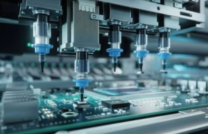
XY axis misalignment : Calibration errors in the vision system, PCB positioning issues (worn locators/loose fixtures) and mismatches between nozzle centers and component centers of gravity may cause partial or complete misregistration. This can lead to cold joints, poor soldering or bridging.
Angular Deviation (θ Rotation). :. Reduced pad area for fine-pitch parts, leading to electrical failures or open joints.
Flip/Inversion : Incorrect feeder installations and faulty library parameter can result in components being placed upside-down or rotated 180 degrees (incorrect polarity).
Impacts: Total functional failure, requiring manual rework. Potential pad detachment due to excessive heat when removing.
3.1.2 Placement Defects
Tombstoning: Uneven solder paste (unbalanced tension during reflow), abnormal placement pressure and excessive reflow temperature will cause chip components with their terminals suspended to stand up on one side, leading to a loss of mechanical strength.
Leaning/Tilting : Coplanarity Failure, Inadequate vacuum pressure can result in component angles >10deg. from PCB surface, (standard =5deg. ), partial pad contacts, semi-wetted joint with reduced vibration resistance and fatigue cracking.
Missing/Excessive placement :Feeder malfunctions or programming errors can result in missing components or duplicate placement on target pads, leading to functional failures or shorts due to duplicates.
3.1. 3 Component Damage and Contamination
Mechanical damage: Excessive placement force and mismatched nozzle sizes can cause body cracks, deformation of lead, and BGA balls to fall out. Latent cracks can reduce reliability over time, while lead misalignment leads to open joints.
Pad contamination : Humidity and feeder track contamination may oxidize terminals or flux residue on component leads resulting in weak joints.
3.1.4 Equipment & Process Anomalies
Nozzle defects:Inadequate cleaning and the wrong nozzle material may cause nozzle clogging and wear.
Feeder Failures: Mechanical wear and improper loading of tape can cause tape feeder jamming, tray feeder misalignment and increased pickup failure rates (>0.5%). This leads to frequent downtimes for recalibration and decreased throughput
Vacuum & Pressure Abnormalities: Miscalibration of the Z-axis pressure sensors and vacuum leakage in the system can cause height deviations for soft-contact components, and terminal indentation on hard-contact parts. Component damage due to excessive pressure. A post-placement shift caused by insufficient pressure.
3.2 Mitigation Strategies
Inspection Methods:
3D AOI identifies placement errors (precision +-15mm), missing components, and polarity errors at >500 components/second.
X-Ray – Verifies BGA/CSP alignement (ball-pad overlap 70% triggers an alarm).
Process control:
First Article Inspection (FAI), using fixtures, measures placement (XYth +-50mm/+-1deg) and verifies 100% of polarity.
Maintenance of the nozzle/feeder: Daily cleaning, 24-hour calibration (precision +-25mm).
Standard Compliance:
IPC-A-610 Class 3: Shift of chip component =25% pad width, leaded component =10% pad length. 100% polarity accuracy.
4.Reflow Soldering stage
4.1 Common Issues
4.1.1 Solder Joint Defects
Bridging :Excessive thickness of solder paste, high peak reflow temperatures, slow cooling rates, and PCB warpage stressing solidification can cause an abnormal solder connection. This leads to circuit shorting and functional failure.
Cold Solder Joint: Reflow temperature below the paste melting point and oxidized component lead, excessive preheat rate and flux volatilization prior to activation result in incomplete wetting of leads and pads, leading to lower joint strength and open circuits during vibration tests.
Solder balls: Paste collapsing during printing, a high oxygen content of a reflow, particles formed by solder oxidation, and an excessive pressure placed on the paste extruding can cause independent solder to form near pads. This could lead to creepage or shorting.
4.1.2 Component Defects
Tombstoning: Volume differences in solder paste on both ends, an asymmetrical reflow profile and a center of gravity misalignment may cause chip components with suspended terminals to stand at one end.
Component shift: Vibrations in the reflow oven and poor paste thixotropy may cause component shifting and edge joint failure.
Component damage: Excessive thermal gradient, moisture absorption, and peak temperature exceeding tolerance can cause MLCC cracks and LED phosphor discoloration.
4.1.3 Thermal Profile Anomalies
Under Preheating: The PCB surface temperature is too high, causing a poor soldering due to the interfacial pressure.
Over-Reflow: Peak temperature duration >60s (ideal 20-40s);
Cooling start temperature >200 may result in PCB substrate discoloration and solder surface oxidation. PCB mechanical strength can be reduced, as well as solder fatigue life.
4.1.4 Equipment & Process Adnormalities
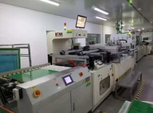
Uneven Heat Circulation : Blocked Reflow Oven Air Ducts and mismatched PCB Size and Chain Width can increase temperature variance within the same batch.
Nitrogen protection failure: Insufficient Nitrogen flow, excessive oxygen concentration and poor oven seal can increase the surface oxide film on solder and cause it to be more porous.
4.1.5 Material & Environmental Issues
Solder paste degradation: Storage temperature >10, (not refrigerated between 2-8), insufficient tempering time 4 hours, and condensation residue may result in an increased viscosity changing rate, higher printing failure, and a reduced thixotropic indices.
Contamination residue: Incomplete cleaning and workshop humidity above 60%RH can cause secondary oxidation, increased flux residues, and decreased long-term reliability.
4.2 Mitigation Strategies
Inspection Methods
Real-Time Profiler: 9-channel board thermocouple (+-1 accuracy) for each shift to ensure compliance with IPC J-STD 003C.
X-Ray Inspection : 3D defect analysis using CT scan, automatic alarm for BGA voids greater than 25%.
AOI+3D: Speed of detection >800 components/second; accuracy in height measurement +-10mm.
Process Optimizer:
Dynamic compensation algorithm: Adjust the preheat ramp speed (1.2-2.5/s), based on PCB thickening (0.8-2.0mm);
Closed-loop nitrogen control: O2 feedback in real-time, ensuring less than 100ppm of O2 in critical areas.
Standard Compliance:
IPC-A 610E Class 3 solder joints: strict coplanarity (50mm), for fine-pitch components with a pitch =0.4mm;
MSD moisture control: automatic dry cabinets for MSL3+ component soldering within four hours of opening.
5. Through-Hole Technology (THT)/Wave Soldering Stage
5.1 Common Issues
5.1.1 Soldering Defects
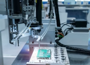
Short Circuit: Excessive solder, incorrect wave height, inadequate component spacing, misaligned lead, or poor flux can cause Electrical short between adjacent leads or pads, resulting in functional failures.
Insufficient Solder/Wetting Deficiency: Inadequate flux coverage, low soldering temperature, short dwell time, oxidized leads/pads, or improper pad/hole design can lead to weak mechanical/electrical connections, and potential open circuits over time.
Cold joints: Rapid cooling or insufficient preheating can result in brittle joints, with a poor metallurgical connection, and are prone to failures.
Solder Voids/Porosity: Trapped flux gases, insufficient degassing when soldering, uneven pad surfaces, excessive moisture in the boards/leads, can all lead to reduced joint mechanical strength and thermal conductivity.
Solder balls: Flux Splatter, improper Wave Turbulence or insufficient post-soldering Cleaning can cause short circuits by stray conductive particle.
5.1.2 Issues Related to Components
Component floating/tilting :Unsecured insertion (loose fitting), insufficient holding forces during soldering or excessive buoyancy can lead to misaligned component, incorrect lead immersion and failed solder joint.
Lead Deformation/Breakage: Excessive insertion force, improper lead forming, or mechanical stress from the wave impact will cause damaged leads, open circuits, or difficulty in subsequent rework.
Thermal damage to components: Excessive preheating temperature, prolonged dwell times, or the use of non-heat resistant components can lead to component failure, reduced lifespan or degraded performance.
5.1.3 Misalignment of Process Parameters
Wave height Improperities:
Too High: Excessive wave impact force can cause component damage and bridging.
Too Low: Incomplete solder contact and insufficient wetting.
Derivations in Preheat Temperature:
Insufficient Preheating: Unsuccessful preheating can lead to poor flux activation and flux residue.
Excessive Preheating: warpage on the board, degradation of solder masks, and component overheating.
Conveyor Speed Mismatch:
Too fast: Reduced dwell times leading to insufficient soldering.
Too Slow: excessive intermetallic compounds, board discoloration, and over-soldering.
Unstable Wave: A dirty solder pot, a pump malfunction or an inconsistent temperature of the tin can cause uneven solder distribution.
5.1.4 Problems Related to Flux
Inadequate Application of Flux : Clogged flux nozzles, incorrect spraying pressure, or improper type of flux can cause poor oxide reduction, reduced wetting and increased soldering defect.
Excessive Flux Residue: Using non-cleanable flux or over-application without the proper processing may result in insulation resistance problems, dendritic formation, or cosmetic defects.
Flux Contamination : Moisture Absorption, contaminants or expired flux will reduce flux activity and compromise soldering performance.
5.1.5 PCB Design & Preparation Issues
Pad/Hole Design Flaws:
Too Small Pads: Resulting in poor solder adhesion as well as mechanical strength.
Incorrect Hole Dimension: Lead fit is too tight or loose, causing solder pullouts and voids.
Uneven Pad Layout: Asymmetrical heat dissipation causing soldering inconsistencies.
Board Warpage: High-temperature exposure, poor-quality PCBs, and improper storage may cause non-uniform contacts with the solder waves, leading to partial soldering, or even open joints.
Incorrect Component Orientation/Position: Human error during insertion, misaligned jigs, or unclear assembly drawings will lead to misplaced leads, soldering onto non-target pads, or interference with adjacent components.
5.1.6 Equipment & Maintenance challenges
Solder Pot contamination : Oxide slag accumulation, metal intermetallic compounds, or inadequate regular cleaning may cause reduced solder fluidity and increase defects.
Nozzle blockages (Flux/Solder Spray Systems): Dust, flux residue or solder balls clogging the spray nozzles may cause an uneven flux deposition or localized failures.
Misalignment of Conveyor Systems: Loose chain, worn gears or vibrations during transport may cause board skew and misaligned parts, as well as inconsistent soldering on the wave contact line.
5.1.7 Environmental Factors
Humidity and Moisture :High ambient moisture or unprotected storage of PCBs can cause pad/lead or flux failure resulting in poor wetting or increased voids during soldering.
Static electricity: Inadequate ESD Protection during component handling/insertion can cause micro-damage. This is more common with SMT than wave soldering.
5.2 Mitigation Strategies
Process control: Regularly calibrate the wave height, temperature and conveyor speed. Use SPI/AOI to automate defect inspection.
Design optimization: Use IPC standards to determine pad/hole sizes and component spacing. Select heat-resistant components in high-temperature areas.
Material management: Store components and PCBs in dry, ESD safe environments. Validate flux compatibility with board finish.
Maintenance Program: Perform routine equipment diagnostics and clean solder pots as per schedule.
6.The Manual Soldering stage
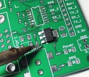
6.1Common Issues
6.1.1 Soldering quality defects (Cold Solder joints, Bridging/Short circuits).
PCB Charring/Pad Detachment: An excessive iron temperature, prolonged heating or repeated soldering at the same joint will cause mechanical damage. Wire jumping is required to fix pad failures; in severe cases, the PCB substrate can be carbonized. This compromises insulation and reliability.
Irregular Solder Joints (Spikes, Solder Balls, Voids): :Oxidized iron tip, which reduces solder fluidity. Premature flux volatilization, or rapid air movements can also cause irregular solder joint. Stress fractures can occur due to insufficient mechanical strength; sharp spikes may cause high voltage arcing and short circuits.
6.1.2 Operational and Component Errors
Polarity/Orientation Errors:Operators who misidentify polarity marks, or ignore work instructions (SOP), can lead to improper lead forming and misorientation when inserting, and, ultimately, failure.
Lead Deformation/Damage:Excessive bend of pliers or iron tip touching non-soldering area; Lead root fractures or in-hole bends can be caused by a forceful insertion.
Thermal Damage to Components: Overheating temperature-sensitive components with prolonged soldering (>3 seconds) or iron tip contacting the body;
The use of non-compatible tips can lead to an excessive transfer of heat. All of them can cause internal structures to fail.
Soldering Wires and Cables Issues: Overheating (melted jackets or broken core wires), missing insulation treatment at solder joints, excessive wire stripping, and overstripping can all cause signal abnormalities, insulation failure or mechanical disconnections.
6.1.3 Tools and Materials Issues
Soldering iron malfunctions: Thermocouple fault in constant temperature irons causes higher temperature deviations from setting, leading to unstable temperatures and inconsistent joint quality. Worn or oxidized tips (lack regular cleaning/tinning), which reduce heat conductivity and increase residue risks.
Incorrect Flux and Solder Use: Mixing of different alloys increases joint brittleness. Using corrosive fluxes without thorough cleansing, or excessive non-clean flux forms insulating layers causing pad corrosion over time. Non-clean residues can cause creepage or interfere with signals.
6.1.4 Deficiencies in Operational and Environment
ESD Control Failures: Ungrounded workbenches or operators not wearing ESD wrist/gloves can lead to electrostatic discharge.
Lead oxidation can occur in components stored in non-ESD bag, resulting from high humidity. This leads to internal breakdown of ESD sensitive components.
Visual Inspection Fatigue: Lack of magnifiers/microscopes for fine-pitch components leads to defect oversight; Prolonged repetitive work without rotation causes visual fatigue and missed micro-defects. Substandard Work Environments: Poor ventilation or inadequate lighting can lead to flux fumes inhalation. Uneven work surfaces may cause uneven insertion forces, component misalignment and indirect soldering defect.
6.2 Mitigation Strategies
Standardized Operation (SOP): Define soldering parameters for different components (e.g. PLCC, DIP), requiring that operators pass a pull-test certification prior to starting work.
Tool Control and Material: Label leaded/lead free stations and replace worn tips every 200 hours (recommended).
Error prevention and inspection: Conduct 100% visual checks and use AOI to check fine-pitch joint joints.
Training & Management: Hold monthly defect analysis meetings. Share case studies (e.g. cold-solder batches returned). Implement a mentor system with mandatory certification for new hires.
7.Inspection and Testing Stage
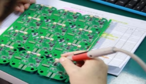
7.1 Common Issues
7.1.1 Visual inspection & Automated Optical Inspect
Undetected Defects and False Positives/Negatives: Improper parameters, insufficient camera resolutions, PCB warpage in the AOI System, operator fatigue when performing manual visual inspections, inadequate training, and substandard lighting are all factors that can lead to surface defects. These defects may then proceed into downstream processes increasing rework and end-user failure risks.
Incomplete Coverage of Inspection: Complex structures and lack multi-angle AOI scan will result in latent defects going undetected.
7.1. 2 Electrical Connection Testing (Flying Probe ICT)
Contact Instability Leading To Misjudgment
Flying Probe Test: PCB Warpage, worn probe tips and oxidized probes.
ICT (In Circuit Test): Unreliable fixture bed of nails (pin pitch tolerance greater than +-0.05mm can cause short circuits); old spring pins.
Test Point design flaws :Design for Test (DFT) omissions and overly dense test point density on test pads.
Misjudgment of Open/Short : Inappropriate threshold setting for the flying probe; ICT not accounting for capacitor/inductor charge/discharging/charging characteristics.
7.1.3 Functional Testing
Reliability Issues with Test Fixtures :Connector failures due to worn spring pins and oxidized fingers, misaligned pin locators, and load boards malfunctions due to drifting simulated loads and distorted waveforms of the signal generator will cause test results instability, frequent recalibration, and possible PCBA damage.
Incomplete test cases: Missing edge cases, omitted co-testing scenarios and software mismatches can lead to undetected defects, such as intermittent crashes or data transmission errors.
Difficulty in Diagnosing: Complex Faults Micro openings in multi-layer/buried throughs and BGA holes missed by X ray require oscilloscope/logic analyser troubleshooting.
High-Voltage/Insulation Test Failures: Reduced surface insulation resistance due to flux residue, insufficient creepage distance (design flaw), or solder bridging between leads, leading to non-compliance with safety standards, risk of leakage or short circuits.
7.1.4 Reliability Testing (Environmental Stress, Life Testing)
Inaccurate stress conditions: Larger temperature fluctuations, unstable humidity control and tri-axial vibrations of Vibration Tables may result in distorted reliability and untrue life prediction.
Unrepresentative Sample: Non-compliant AQL testing and sampling non-representative batch (e.g. only first article inspection, equipment drift missing in mass production). This will cause systematic defects to be undetected.
7.1.5 Data Management & Process Issues
Isolated Data: Unintegrated AOI/ICT/functional Test Data and requiring more than 30 minutes per defect can delay the identification of bottlenecks in the process.
Non Uniform Standards:Inconsistent standards can lead to repeated inspections and omissions. Quality disputes are frequent, as well as ambiguous rework standard.
Operator error: Deviation from SOP, and accidental probe contact can result in direct component damage.
7.1.6 Limitations of Equipment and Technological Development
Blind Spots in Emerging Processes :Micro Joints (0.3mm pitch): Insufficient traditional resolution of AOI; X-ray scanning time per board >2 minutes, low efficiency.
Embedded components/3D packages: Unreachable internal connectors for conventional testing. Relies on destructive tests.
Latent defect omission: Internal cracks in solder joints only visible with long-term vibration; undetected through static tensile tests. Micro-shorts due to ion migration require >72 hours high-humidity, above and beyond normal testing.
7.2 Mitigation Strategies
Proactive DFT: Standardize test point designs during PCB layout in order to eliminate blind spots for inspection.
Intelligent Data Integration: Deploy interconnected AOI/X-ray/ICT/functional test systems with AI correlation.
Dynamic Standard Calibration: Update detection thresholds using historical yield data to avoid over/under-tolerance.
Workforce certification: Implement IPC-A-6610 certification for inspection roles, fatigue management.
8.Cleaning & Conformal coating Stage
8.1 Common Problems
8.1.1 Incomplete cleaning leading to contamination residue
Flux residue: Improper cleaner selection and insufficient cleaning temperature/time, as well as obstructions by complex geometries, will cause electromigration failures over the long term. Rosin acid reacts to moisture, creating corrosive substances that accelerate solder joint/copper corrosion.
Ionic Contaminant Residues:Inadequate rinsing with deionized and recycled water in aqueous cleaning can cause electrochemical migration. Ionic contamination above IPC-A610 limits increases the failure risk.
8.1. 2 Material and Chemical Incompatibility
Metallic coating corrosion : Alkaline cleaners, pH >9, discolor pure tin/silver coatings. Gold-plated connector pins that are corroded increase contact resistance and can cause signal transmission problems. Nickel pad corrosion decreases solder joint adhesiveness, which increases the risk of cold solder.
Damage to non-metallic materials: Strong polar solvents dissolve the solder masks. Ultrasonic cavitation causes cracks in adhesive/underfill. Solder masks that are damaged expose copper and reduce creepage distance. Silk-screen labels/legends dissolve.
8.1. 3 Physical and Mechanical Defects
Mechanical stress on Components/Soldering Joints: Over-spray pressure can displace components (>50% pad shift, requiring rework); Incorrect ultrasonic frequency may cause electrolytic capacitor lead fracture fatigue. QFP lead deformation due to cleaning fluid impact. BGA ball microcracks caused by vibration stress.
Substrate Damage to PCBs: Poor fixture design, high temperature cleaning and abrasion of the multi-layer resin can lead to micro-cracks.
8.1. 4 Improper Drying Leading To Secondary Defects
Moisture retention:Insufficient drying by hot air and a short drying time can cause water to accumulate under components causing pad rust. Freezing moisture during thermal cycling (-40°C) will expand by 9%, which may crack solder joints.
Foreign particle adhesion :Failed filters in dry systems can cause insulating particles contaminants to cause flashovers in high-voltage module.
The rhombic crystals formed by hard water (calcium/magnesium in the solution) can scratch precision components.
8.1. 5 Failures of Process Parameters and Equipment
Cleaning equipment anomalies: Ultrasonic transducer failure, spray pump clogging and cleaner batch mixing can all be caused by cleaning equipment malfunctions.
Process Deviations: Ignoring cleaner replacement cycles doubles contaminants concentration; overloaded cleaning baskets decrease fluid exchange efficiency
8.1.6 Inadequate Inspection and Validation
Insufficient Cleaning Testing:Only Visual Inspection, Missing Latent Residues (Requires Ion Chromatography for ionic Contamination);
No real-time SIR monitoring (insulation degradation undetected under dynamic >100V testing).
Conflicts between Standards:Internal Standards allowing minor rosin residues vs. IPC A-610 Class 3 requiring completely residue-free surfaces.
Rework cleaning risks: Non specified solvents and repeated washing will cause secondary damages.
8.2 Mitigation Strategies
Selecting a Cleaner: Match cleaners with flux chemistry. Aqueous cleaning is controlled by conductivity of 5mS/cm2 and pH between 6.5-7.5.
Process optimization: ComplexPCBs are “pre-spray+ultrasonic+double-rinse”, with mechanical vibrations (20-30mm for blind spots); Combination hot air/vacuum drying (85%+-5%) ensures complete moisture evaporation in microvias.
Reliability of Equipment: Daily calibration for spray power, ultrasonic and temperature uniformity, (deviation +5%); AOI upgrade using 3D structured-light scanning for 0.1mm particles detection.
Testing & Traceability: Quantitative metrics: SIR >1012O at 50V DC and 25/60%RH; MES system records batch parameter (time, temperature, lot number of cleaner) for full tracability (to PCB serial numbers).
8.3 Conformal Coating Common Issues

8.3. 1 Coating Uniformity and Thickness Defects
Uneven Distribution of Coating:nozzle blocking in spray coating and improper control surface tension can cause thin coatings (ASTM B117 test) to fail within 24 hours and thick coatings mating failures.
Bubble and Void Formation: Trapped Solvent in Thermal Curing and Poor degassing can cause voids in corners of BGAs, exposing solder balls and RF traces to moisture.
8.3. 2 Adhesion & Coating Material Compatibility Issues
Metallic Surface reactions: Silicone coatings react with surfaces that are silver-plated; acrylic coatings erode nickel layers. Corroded pads reduce reworkability. Intermittent electrical contact is caused by delaminated coatings on gold fingers.
Nonmetallic Material Interactions: Epoxy Coatings Shrink During Cure, causing cracks on component edges. Aggressive Thinners Dissolve Silk-Screen Inks, Making Component Identification Impossible.
8.3. 3 Coverage Defects and Process Overspray
Critical Omission: Improper masking or low-pressure coating fails to penetrate dense lead spaces in QFP (pitch less than 0.5mm), causing uncoated contacts to corrode when sprayed with 5% NaCl and exposed via holes that allow flux residue to absorb, leading to SIR failure after post-coating.
Overspray and Foreign Matter Inclusion: Inadequate enclosed during spray coating, and static attraction to uncured coatings may result in insulating particle between high-voltage tracks (creepage failure >200V; IPC-2221A creepage space violated), and overspray onto optical components.
8.3.4 Curing Deficiencies & Performance Degradation
Incomplete cure: Thermal curing at temperatures below the specified temperature or insufficient UV exposure may lead to coatings that are not cured and absorb moisture, and can cause mechanical failure.
Thermal Stress & Over-Curing: Excessive temperatures and long dwell times in curing ovens (>2 hrs at 150 induce coating brittleness). Thermal cycling can cause coatings to crack and chemical resistance will be reduced.
8.3. 5 Process Control & equipment Anomalies
Variable Coating Thickness: Pump Pressure Fluctuations (affecting Spray Volume) and Nozzle to PCB Distance variations can cause thickness nonconformance with IPC-CC-830 class 3 requirements.
Errors in Masking and Defluxing:Incorrect application of mask due to human factors, or forgetting to remove the mask will result in a coating on grounding pad (ground impedance increases >20mO).
8.3.6 Combination of Cleaning and Coating Process Interactions
Coating Defects Caused by Residues: Flux residua act as release agents and cause coating delamination.(peel test failure at residues, adhesion strength reduced by 70%).
Impact of Over-Cleaning on Substrates: Excessive Cleaning weakens the surface roughness. (Ra <0.5μm reduces coating mechanical interlock, adhesion failure risk up).
8.4 Mitigation Strategies
Material selection: Match coating chemistry with substrate/finish.
Process optimization: Use automatic optical inspection (AOI), with 3D thickness maps for critical areas. Implement pre-coating Plasma treatment.
Reliability Tests: Combined thermal cycling and SIR test; cross-sectional analysis of the coating-substrate (SEM-EDX), for the integrity of the interface between substrate and coating (checking intermetallic formations or voids).
9. Post-Assembly and Curing Stage
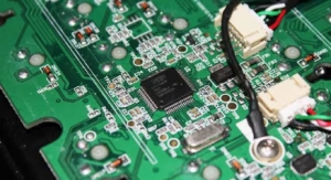
9.1 Post-Assembly Common Issues
9.1.1 Component damage from mechanical assembly stress
Micro-cracks on rigid components caused by fastening/crimping stresses;
The pad may lift due to excessive mating force.
9.1. 2 Connector Assembly and Interconnect Assembly Defects
Contact and Misalignment Issues : Mechanical position errors can cause pin bending, gold finger oxidation and a bit-error rate (BER>10-9) for high-speed differential signal due to an impedance mismatch and local overheating caused by poor power connector contacts.
Solder Residue & Insulation Failure: Ionic flux residue greater than 1.5mg/cm2 equivalent NaCl, leading to creepage
The PCB can be micro-deformed or even fractured by excessive cable bundling (>10N/cm2).
9.1.3 Thermal Mismatches and Structural Mismatches
Heat sink bonding defects:Uneven thickness of thermal paste and inconsistent screw torque may lead to CPU junction temperatures exceeding 125 (halving service lifetime) and increased thermal resistance in power module triggering overload protection.
Structural interference with PCB:Hidden cracks in pad due to excessive EMI shielding pressure; PCB warpage greater than 0.7% (IPC A-610 Class 2 Allowable Value) caused by plastic clip stress.
9.2 Post-Assembly Mitigation Strategies
Integrate automatic screw torque monitoring (accuracy ±3%, real-time data logging);
After connector assembly, perform continuity and contact resistance scans (0.1mO Resolution).
9.3 Curing Common Problems
9.3. 1 Adhesive Curing Inadequate and Performance Defects
Curing Anomalies: Errors in temperature profiles and mixing ratios can cause stress concentration and an inadequate solder ball buffering.
Potting compound cure defects:Unremoved bubbles reduce partial discharge voltage at inception. Bubble discharge can cause insulation failures in high voltage modules (>1kV). Delay cure at low temperature can cause interface separation and moisture-induced corrosion.
9.3.2 Conformal Coating Curing Defects
Solvent Remains in Solvent Based Coatings:Inadequate airflow in the convection oven delays solvent evaporation. Short drying times between layers trap solvents. Solvent erosion on sensitive components. Long-term VOC emissions causing sensor drift.
Incomplete Curing: Incorrect UV wavelengths resulting in energy loss and excessive conveyor speeds will result in an irritated surface with reduced chemical resistance.
9.3.3 Material Compatibility during Curing
Adhesive Surface Finish Reactions:Chelation between amine hardeners (hardeners) and metal surfaces to increase contact resistance
Increased potential difference between ENIG & curing accelerators.
Substrate warpage and Shrinkage Stress: High-modulus adhesive shrinkage of >1%, and the lack of stress-relief channels in large-area potting causes solder joints to crack in fine-pitch component and PCB warpage.
9.3.4 Process Control and Equipment Abnormalities
Uneven Curing Field Temperature:Increased Zone Temperature Variation and Aged Infrared Heaters can cause Glass Transition Temperature Blow Target and incomplete Coating Removal during Rework Per IPC-7711/7721 Standards.
Deviation in Dispensing Volume:Increased Air Pressure Fluctuation and Worn Nozzles causing Adhesive Overflow can result in incomplete BGA Edge Coverage and Pad Contamination from Excessive Dispensing leading to Poor Solder Wetting.
9.3. 5 Interaction between assembly and curing
Assembly residue impact on curing:Fingerprint/oil contaminants cause coating craters. Metallic debris embedded into cured layers forms conductive paths.
Curing defects affecting assembly: Uncured adhesive sticks to fixtures and causes PCB tear; Uneven hardness of cured material leads to component misalignment.
9.4 Curing Mitigation Strategies
Material and Process Matching: Select UL94 V-0-rated potting compounds. Use silicone gels in high-temperature environment (>180). Conduct flowability testing for underfill.
Process control: Equip curing ovens and dispensing thickness inspectors with laser profilers.
Validation of Reliability: Perform DMA (Dynamic mechanical analysis) to measure Tg, storage modulus and conduct vibration testing to verify the mechanical reliability.
10.Packaging Stage
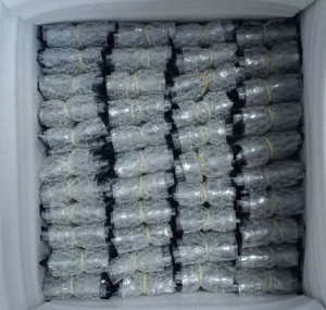
10.1 Common Issues
10.1. 1. Inadequate packaging materials and protection
ESD/Moisture Protection Failure:
Incorrect material selection: Failure to use ESD protective bags, moisture proof bags, or cushioning materials that comply with ESD regulations, leading to ESD damages during storage/transport, or moisture ingress.
Sealing defects: Insufficient desiccants or humidity indicator cards (HICs) that fail to block moisture. Damaged or incompletely-sealed ESD bags that compromise electrostatic protection.
Insufficient mechanical protection:
Lack of cushioning: Low-quality or missing foam padding can cause component detachment or PCB deformations (bending/fracture) or bent connector pins as a result of vibrations or impacts during transit.
Improper stacking: Lacking separator plates when stacking multi-layer PCBA or overloading packaging containers can lead to bottom-board deformation and compression.
10.1.2 Labeling Issues
Labels that are incorrect or missing
Information errors: Labels that have mismatched content, or barcodes/QR code that are unreadable can cause confusion in warehouse management and lead to customer rejection.
Label placement: labels covering mounting holes, test points or silk-screen marks, preventing subsequent assembly or repairs; blurred/skewed labels that reduce readability.
Incomplete Data for Traceability:Failure of packaging-related production batches to be recorded, inspection status or other data or falling off the traceability label, making it impossible to analyze quality issues and violate ISO or customer-specific requirements.
10.1. 3 Operational non-compliance and human errors
Process Deviations:
Mix-ups/Misbatches : PCBs from different batches/models are mixed in one package. Or, the good boards and reworked boards are not separated as needed, resulting in delivery errors.
Foreign Object Contamination : Dust, solder slag or forgotten tools such as gloves or tweezers left in the packaging can cause short circuits and cosmetic defects.
Mechanical damage risks:
Rough handling: Excessive force used during manual packaging can cause lead deformation, PCB edge chips, or pad detachment.
ESD Protocol Violations – Operators don’t use ESD wrist/gloves, or workbenches that are not grounded. They also directly touch PCBA surfaces causing ESD damage.
10.1. 4 Environment and Storage Risks
Failures in Temperature/Humidity control:Packaging with high humidity and no moisture-proofing measures leads to pad/lead corrosion; packaging at high temperatures accelerates the aging of plastics or component degradation.
Hazardous contamination:Use non-environmentally-friendly materials, in violation of RoHS/WEEE regulation; volatile gases produced by low-quality foam that corrodes PCBA surface coatings.
10.1.5 Problems with Equipment and Automation
Packaging Equipment Failures:
Precision Issues: Misaligned labeling machines resulting in skewed or unreliable labels, or incorrect coverage of critical areas. Defects in sealing machine temperatures/pressures resulting loose seals or bag damage.
Mechanical Damage: PCB edge or component displacement caused by excessive gripping force of robotic arms, uneven conveyor speeds, or collisions on automated lines.
Software System Errors:
Failures in MES data synchronization leading to mismatches between label production records and labels; and errors in automated equipment programs omitting crucial protective materials.
10.1. 6 Gaps in Compliance and Customer Requirements
Custom Requirements Unmet: Failure to adhere to customer-specific packaging requirements (size, shock resistant, labeling format, etc.) resulting in batch return.
Certificate Deficiencies: Packaging Materials Lacking Safety Certifications: Packaging Materials lack the necessary safety certifications.
10.2 Mitigation Strategies
Material Control: Use ESD/moisture-certified packaging materials, regularly testing properties.
Standardization of Processes:Define detailed Packaging SOPs including label content and protection steps; implement error-proofing to prevent labels/mix-ups (e.g. barcode verification).
Training of the workforce: Regularly train operators in ESD protection, equipment operation and certification before independent work.
Equipment Maintenance: Establish calibration/maintenance schedules for automated packaging equipment, recording operational parameters (e.g., label position, sealing temperature).
Environment Monitoring:Deploy electrostatic voltage testers and thermohygrometers in packaging areas to record real-time conditions.
Traceability from start to finish: Link packaging data (batch ID, operator ID, equipment number) via MES. This ensures full traceability at all stages of production.

11.Summary
PCBA problems are primarily caused by process deviations, incompatibility of materials, instability of equipment, and human errors. Standardized operations, statistical process control (SPC), first-article inspections (FAI), and automated tests (AOI/X-Ray) are required to mitigate.
Contact Us
Phone: +86-18123905375
Email: sales@assemblepcb.com
WhatsApp: +86-18123905375
Wechat: +86-18123905375
Free Queto
Latest Blog
Table Of Contents
Contact Us
Phone: +86-18123905375
Email: sales@assemblepcb.com
WhatsApp: +86-18123905375
Wechat: +86-18123905375
Free Queto

