What is the process for PCB assembly
Table Of Contents
We meet electronic devices on a daily basis, but are you aware of their fundamental parts? The answer will now be explained in this article. PCBs are what they are. However, PCB alone cannot transform into the electrical items we see; at this moment we need to comprehend PCB assembly.
PCB assembly (printed circuit board assembly) is a complex process that combines parts and ensures reliable electrical connections to turn blank PCBs into working electronic modules. Additionally, this essay will introduce you to the fascinating process of PCB assembly.
1.PCBA Design Phase and Preparation
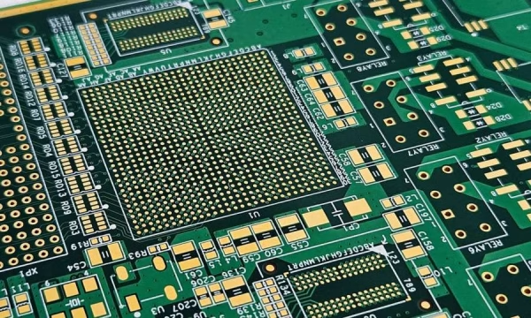
(1)Gerber Files: Define PCB layers (copper traces, solder mask, drill holes, silkscreen).
(2)Bill of Materials(BOM): List components such as resistors and ICs. Confirm their part numbers, quantity, and supplier.
(3)Assembly drawings: Specify component location, orientation, special instructions, and more.
(4)DFM Check: Verify component spacing, pad sizes, and thermal control to avoid manufacturing defects.
(5)Stencil Design: Laser-cut stencils for solder paste printing.
(6)Test Fixtures: Design FCT (Functional Test), ICT (In Circuit Test) and align the fixtures with test points.
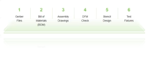
PCBA Design Phase and Preparation
2.PCBA Material Preparation & IQC (Incoming Quality Control)
2.1 Material preparation
(1)Fabrication of PCBs (if they are not pre-fabricated).
Substrate selection: Materials such as FR-4 or high-temperature materials, which are used for general purposes, are cut into panel-sized boards.
(2)Component Source: Procure components (SMD/THT), ensuring compatibility and quality.
(3)Polarity and Labeling: Verify polarity markings & lot codes for traceability.
(4)Solder Paste and Adhesives: Select the solder paste for your specific application.
2.2 Incoming Quality Control (IQC)
(1)Continuity Testing: Flying Probe Testing to verify electrical connection.
(2)Visual Inspection: Check the solder mask for defects (bubbles and peeling).
(3)Electrical Performance: Test capacitors, resistors and ICs using LCR meters.
(4)Surface Finish: Validate ENIG thickness (Electroless nickel immersion gold) or HASL thickness (Hot Air Solder leveling).
(5)Mechanical Integrity: Inspect connectors, THT pins, and other mechanical components for deformation or bending.
(6)Material Composition: Use an XRF machine to verify alloy ratios and lead-free compliance.
(7)Packaging and ESD Protection: Check moisture barrier bags (MBBs) for seals and humidity indicator cards.
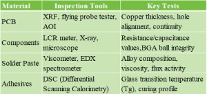
Material Inspection Tools Key Tests
3.PCBA Surface Mount Technology (SMT) Assembly Phase
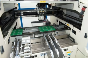
3.1 Solder Paste Printing
(1)Stencil inspection: Assess the dimensions of the stencil openings, their cleanliness and tension before solder paste is printed.
(2)Solder Paste printing: Using a squeegee, solder paste—a blend of flux and alloy powders—is applied to the pads after a stencil has been aligned with the PCB.
(3)Solder Paste Inspector (SPI): To avoid soldering flaws, check the quality of the solder paste.
3.2 Component Placement
Pick and Place Machines: Resistors and capacitors are picked up by high-precision machinery on feeders and then placed on solder paste that has already been printed.
3.3 Reflow soldering
(1)Pre-Reflow Automated Optical Inspection (AOI): Use an AOI to verify each component’s location, type/value, and polarity before reflowing it.
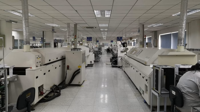
(2) Reflow Oven: PCB is subjected to a controlled thermal pattern (typically 5 zones: preheating, soak, reflow and cooling) in order to melt solder paste. Solder melts, forming reliable joints.
3.4 Inspection after Reflow
(1) Post-Reflow Automatic Optical Inspection(AOI): Surface Mount Defect Detection (like missing components or reversed polarity).
(2) X-Ray Inspection: Examine the Through-hole Fill and BGA/QFN joints.
(3)SMT First Article Inspection (FAI): SMT Verify if the PCBA assembled in the first assembly is correct before mass production.
(4) Monitoring of the reflow temperature profile: Check that the temperature profile in the soldering oven meets the requirements for solder pastes and components.
(5)Process quality control (IPQC): During the PCBA key process, inspect samples in real time.
(6)In-circuit test (ICT): Use a flying probe tester to check the connection of the circuit. Every product that has flaws is fixed.
4.PCBA Through-Hole Technology (THT) Assembly Process
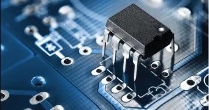
4.1 Component Insertion
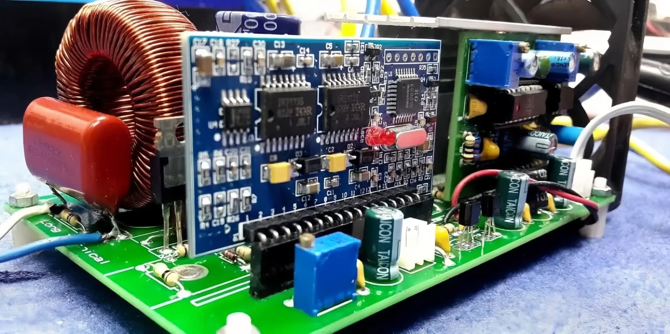
Manual/Automated Insertion: Through-hole components (e.g.,connectors, inductors, etc.) with lead pins can be inserted manually or by radial/axial inserting machines.
4.2-Wave Soldering
(1)Prewave Automated optical inspection (AOI): Just as with reflow soldering, use an AOI for component placement.
(2) Soldering Wave: PCBs are passed over a wave of molten solder, coating the pins and creating connections.
(3)Postwave Automated optical inspection (AOI): Similar to reflow assembly, AOI compares images to learned images after assembly. All detected failures will be subjected to a manual review and the defective unit(s) will be put aside for repair or analysis.
4.3 Soldering Manual
Manual soldering: Wires, and other non-washable components that must be soldered with a dedicated machine. After cleaning the circuit board of flux residue, a technician can solder the wires by hand.
In your PCB assembly notes, you can specify the soldering technique for parts with sensitive through-holes.
4.4 Post-Soldering Processing
(1)Lead trimming: Retain a 1.5-2mm length of lead to prevent solder joint damage.
(2)ESD Safety: Use grounded tools to protect components.
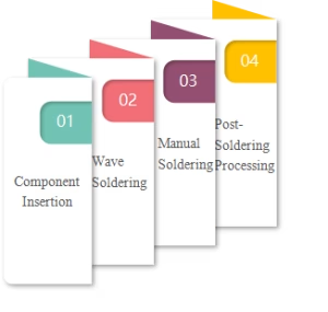
PCBA Through-Hole Technology (THT) Assembly Process
5.PCBA Post-Assembly Processes
5.1 Cleaning
Cleaning: Remove flux residues with water-based or solvent-based cleaners.
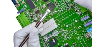
5.2 Final inspection & validation
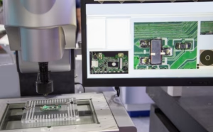
(1)Inspection
Visual inspection: Check component misalignment or coating flaws.
X-ray Inspection: Verify through-hole fill rates of greater than 75% and BGA/QFN solder junctions.
(2)Validation
Functional Test (FCT): The assembled PCB is powered up and tested in real-world conditions.
Environmental Stress Testing (ESS): Temperature cycling to reveal potential flaws.
Burn-In Testing: Operating Constantly at High Temperature for a Predetermined Amount of Time to Spot Early Failures.
5.3 Conformal coating
Conformal Coating: Use silicone or acrylic coatings to protect against corrosion, moisture, and dust.
5.4 Curing and Encapsulation
Curing/Encapsulation: For endurance, enclose delicate parts or cure adhesives.
6.PCBA Rework & Repair Phase
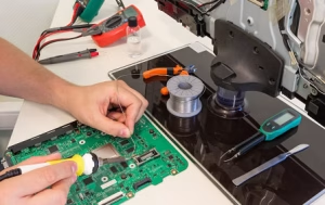
6.1 Rework & Repair
(1)Defect resolution: Failed joints or components are removed with a hot air rework station (for SMDs) or desoldering pump (for THT). New components are repositioned and then reflowed.
(2)Desoldering Wick/Tools: Remove excess or bridge defects.
(3)Post-rework testing: Re-validate electrical performances and coating integrity using ICT or FCT.
(4)X-ray: Verify the through-hole fill and BGA void rate.
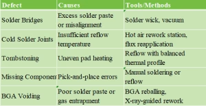
Common Defects Requiring Rework
6.2 Documentation & Traceability
(1)Rework logs :Record defects and repair steps as well as post-repair testing results.
(2)Traceability: Tag boards that have been reworked with unique identifiers to track quality.
6.3 Labeling and Marking
(1)Laser marking: Impress serial numbers, date code, or compliance logos such as UL, CE.
(2) Labels: ESD Warnings, RoHS Compliance, and Barcodes for Traceability.
7.PCBA Packaging and Shipping Phase
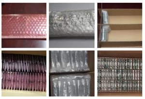
7.1 Shipping & Packaging
(1)Protection against ESD: Anti-static bags with moisture indicator cards
(2) Mechanical Protection: Custom foam inserts or vacuum-formed trays to protect against vibration damage.
(3)Documentation: Include test reports, certificates (CoC) of compliance and assembly records.
(4)Bulk Packaging:
Boxes: Corrugated cardboard with ESD safe liners.
Pallets: Stack the boards vertically in order to avoid bending (maximum height 1.5m).
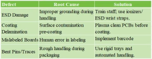
Common Defects & Solutions
7.2 Documentation & Traceability
(1)Test reports: Include results of ICT/FCT/AOI/Xray.
(2)Certificates Of Conformance(CoC): Confirm compliance with RoHS, Halogen-Free, REACH or other standards.
(3)Tracability: QR code are linked with Production date, batch numbers, Component lot codes for recalls, Test data and rework histories.
8.FAQs
1) How do we optimize the cost and quality of PCBA?
High-Volume Production: Prioritize automated tests (AOI, IT) to speed up production.
Low-Volume/Prototypes: Focus on FCT and manual inspections to reduce upfront costs.
2) How many cleaning methods are available in PCBA?
Three methods are available:
Solvent cleaning for rosin based fluxes;
Aqueous Cleaning is an eco-friendly, water-based solution for cleaning fluxes that are difficult to clean or have low residue;
Ultrasonic cleaning is also available for complex boards that have tight component spacing.
3)How are conformal coatings classified in PCBA?
There are three types: acrylic, silicone, and urethane.
4) What is the difference between PCB and PCBA?
PCB is a substrate that has not been populated.
PCBA (Printed Circuit Board Assembly) is a board that has soldered components.
5)What is the process of PCB assembly?
Six steps are usually involved in the main steps:
Step 1: Prepare: Validation of the design, procurement of components, and inspections on bare boards.
Step 2: SMT assembly: Component placement – solder paste printing – reflow-soldering.
Step 3: THT Assembly if necessary: Component insertion and wave soldering.
Step 4: Inspection and testing: AOI/X ray for solder joints; ICT/FCT functionality; Manual Inspection for defects in visual appearance, IPQC process sampling.
Step 5: Rework and Reliability Testing: Defect repair and environmental/stability testing.
Step 6: Finishing: Labeling, anti-static packaging, protective coating and finalization.
6) Manual insertion or automatic insertion is better for PCB THT assembly?
Both have their advantages. It depends on the production requirements, component properties, batch size, and cost goals to determine which is better.
7)Should you choose auto-insertion or manual insertion for the PCB THT Assembly?
Manual Insertion: Manual Insertion is used for low-volume production and irregularly shaped parts.
Auto-Insertion: large production or regular, standardized parts.
8) Does PCB assembly require conformal coating?
It is not necessary to apply conformal coating everywhere. It is important when PCBs need to be highly reliable and are exposed to harsh environments.
9) How to use X-Ray Inspection during PCB Assembly?
X-ray inspection is required for assemblies involving hidden components (BGAs, CSPs, flip-chips), industries with high reliability, and critical processes.
10) What is a PCB Assembly Drawing?
A PCB Assembly Drawing is a technical document that provides detailed instructions on how to assemble components onto a printed-circuit board (PCB).
9.Summary
The PCB assembly is a complex process that involves a lot of steps. Employing a group of experts is crucial.
ORINEW Technology CO., LTD has been a PCB Assembly Manufacturer for over 12 years. We offer a one-stop PCB Assembly service that is high quality and low cost with competitive capabilities. ORINEW can provide you with more information on PCB manufacturing.
Contact Us
Phone: +86-18123905375
Email: sales@assemblepcb.com
WhatsApp: +86-18123905375
Wechat: +86-18123905375
Free Queto
Latest Blog
Table Of Contents
Contact Us
Phone: +86-18123905375
Email: sales@assemblepcb.com
WhatsApp: +86-18123905375
Wechat: +86-18123905375
Free Queto

