
SPI in PCB Assembly: Your Guide to Zero-Defect SMT
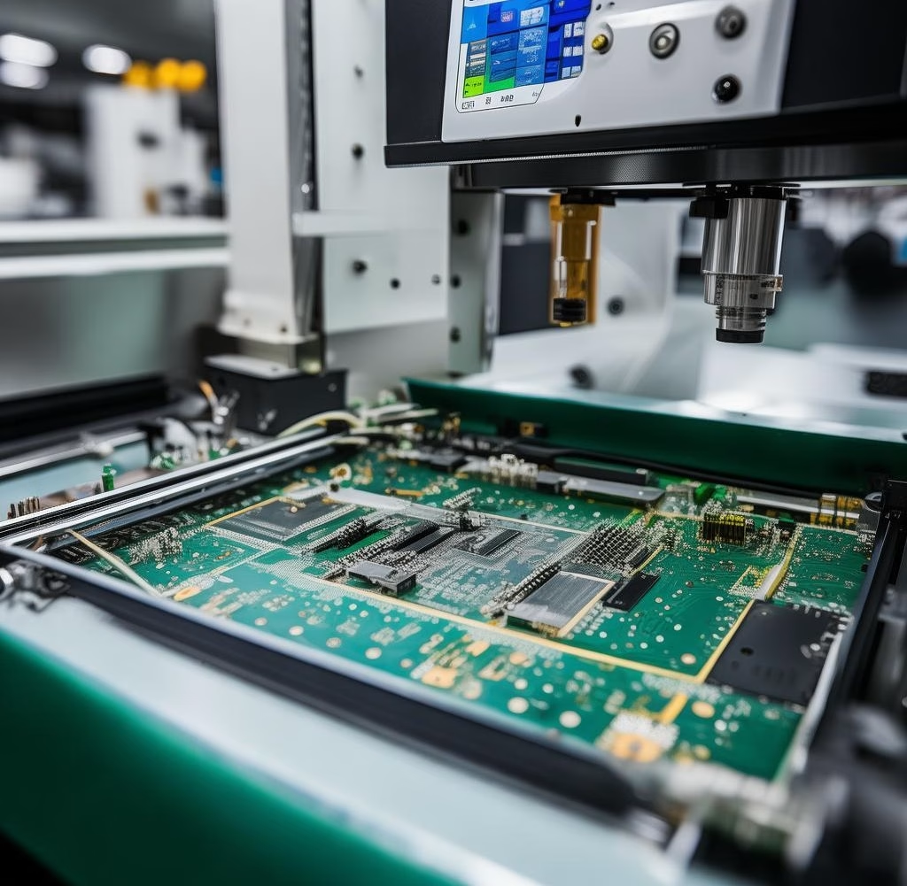
Table Of Contents
1. The Unsung Hero of SMT Quality
In the intricate world of Printed Circuit Board Assembly(PCBA), precision is paramount. Every component, every connection, and every microscopic bead of solder paste contributes to the final product’s functionality and reliability. While many focus on the dazzling array of components or the complex routing of traces, one critical step often operates behind the scenes, yet prevents up to 70% of potential defects: Solder Paste Inspection(SPI). Studies reveal that a staggering 80-90% of defects in Surface Mount Technology(SMT) assembly originate from the solder paste printing phase. This makes the accuracy of solder paste application not just important, but absolutely fundamental to achieving high-quality, cost-effective electronics.
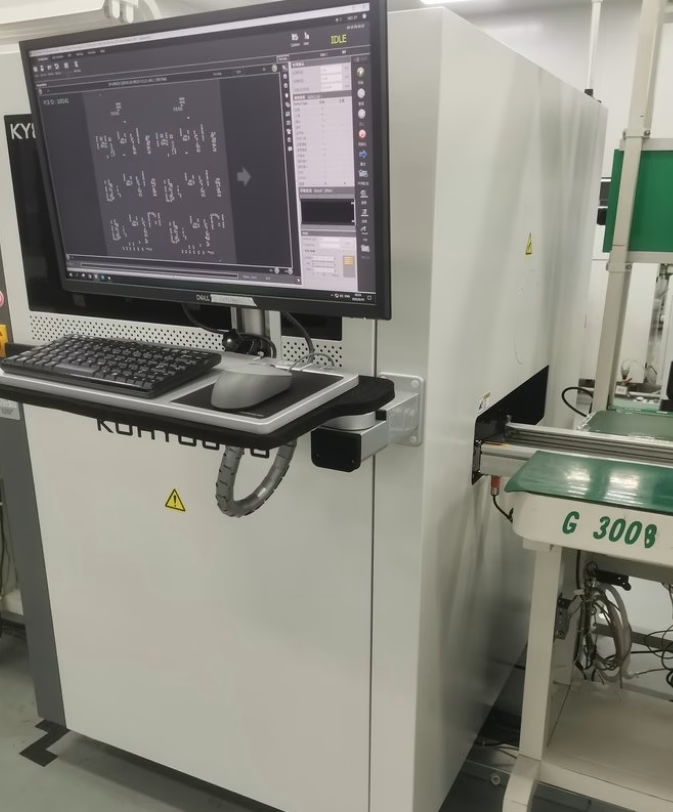
Imagine the cost of an undetected flaw. A tiny error in solder paste application, perhaps an insufficient volume on a critical pad, can lead to a device failing in the field. This “undetected defect” can cost 10-100 times more to resolve than catching it on the production line, incurring warranty repairs, logistical nightmares, and significant reputational damage. This economic reality underscores the vital role of SPI. By acting as a strict “quality guard” immediately after the solder paste printing, SPI ensures that any issues are detected and corrected early, drastically reducing rework costs and enhancing product reliability. As components become smaller and more complex, such as 0201 packages, the importance of precise solder paste inspection only continues to grow.
2. What is Solder Paste Inspection(SPI)?
Solder Paste Inspection(SPI) is an automated optical inspection technology used in the SMT assembly process to measure the volume, area, height, and alignment of solder paste deposits on a PCB. It is strategically placed in the assembly line directly after the solder paste printing machine but before the component placement machine(pick-and-place). This placement is crucial because it allows manufacturers to identify and correct solder paste defects before expensive components are placed and before the board proceeds to reflow soldering, where defects become significantly harder and more costly to fix.
The primary goal of SPI is to verify that the solder paste has been applied correctly, adhering to precise specifications. It’s not just about presence or absence; it’s about the exact three-dimensional characteristics of each paste deposit. By validating these parameters, SPI ensures that each joint will form a robust electrical and mechanical connection during reflow, preventing issues like opens, shorts, or weak joints.
3. Why SPI is Indispensable for SMT Quality and Cost Savings?
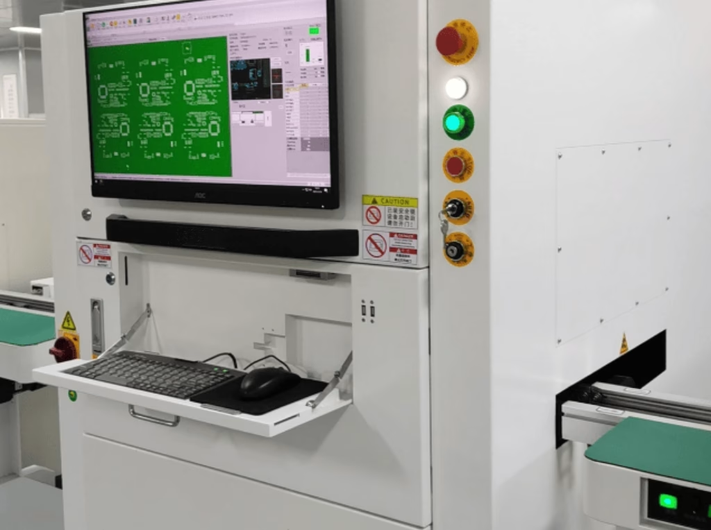
The economic and quality benefits of integrating SPI into the PCB assembly line are profound. It acts as a proactive defense mechanism against the most common source of SMT defects, offering a high return on investment through several key advantages:
- Early Defect Detection:As noted, the majority of SMT defects originate from the solder paste printing process. SPI catches these issues at their earliest stage, preventing them from propagating further down the line. Correcting a paste defect is as simple as washing the board and reprinting; correcting a defect after reflow might involve complex, time-consuming, and potentially damaging rework.
- Significant Cost Reduction:The cost to fix a defect escalates dramatically at each subsequent stage of manufacturing. A defect identified by SPI can be addressed for pennies compared to dollars if found after component placement or tens/hundreds of dollars if found after reflow. If a defect reaches the customer, the cost can be thousands. SPI thus saves substantial money on rework, scrap, and warranty claims.
- Improved Product Yield:By ensuring the quality of solder paste application, SPI directly contributes to a higher first-pass yield, meaning more PCBs are produced correctly the first time. This optimizes production efficiency and reduces material waste.
- Enhanced Product Reliability:Consistent and accurate solder paste deposits lead to stronger, more reliable solder joints. This is crucial for the long-term performance and durability of electronic products, especially in critical applications like automotive, medical, or aerospace.
- Process Optimization and Control:SPI systems provide valuable data about the printing process. This data can be used for real-time feedback to adjust the solder paste printer, implement closed-loop process control, and identify trends that might indicate issues with the stencil, squeegee, or paste itself. This continuous improvement is a hallmark of lean manufacturing.
4. How Modern SPI Technology Works: Unveiling the 3D Advantage
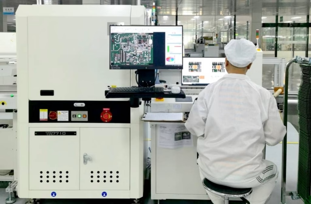
Modern SPI systems primarily rely on 3D measurement technology to accurately assess solder paste deposits. While older 2D systems could detect the presence and area, they struggled with critical parameters like height and volume, which are vital for reliable solder joints. 3D SPI overcomes these limitations by generating a detailed topographical map of each paste deposit.
Key Principles of 3D SPI:
- Light Projection:The system projects structured light patterns(e.g., fringe patterns, laser lines) onto the solder paste and PCB surface.
- Image Capture:Multiple cameras capture the distorted patterns reflected from the surface. The way the light patterns are distorted provides information about the height and shape of the paste.
- Triangulation and Reconstruction:Using principles of triangulation, sophisticated algorithms reconstruct a precise 3D profile of the solder paste deposit. This allows for accurate measurement of all critical parameters.
Critical Solder Paste Parameters Measured by SPI:
| Parameter | Description | Importance for Solder Joint Quality |
| Volume | The total amount of solder paste deposited. | Crucial for proper metallurgical connection and prevention of opens or shorts. |
| Area | The footprint of the solder paste deposit on the pad. | Affects bridging potential and solder joint strength. |
| Height | The vertical dimension of the solder paste deposit. | Directly impacts solder joint volume; critical for proper standoff and component alignment. |
| Offset/Alignment | The positional accuracy of the paste relative to the pad. | Misalignment can lead to tombstoning, shorts, or weak joints. |
| Shape/Bridging | The contour and separation between adjacent paste deposits. | Detects unintended connections(shorts) between pads. |
5. Common Solder Paste Defects Detected by SPI
SPI systems are adept at identifying a wide range of solder paste defects that can compromise the integrity of the final product. Here are some of the most common issues they catch:
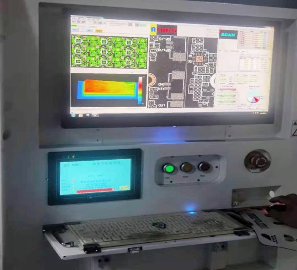
- Insufficient Solder Paste: Too little paste can lead to “open” circuits or weak solder joints.
- Excessive Solder Paste:Too much paste can cause “bridging”(solder shorts) between adjacent pads, especially on fine-pitch components.
- Misalignment/Offset:The solder paste deposit is not accurately centered on the PCB pad, leading to potential tombstoning or poor self-alignment during reflow.
- Smearing:Solder paste spread unintentionally onto the solder mask or between pads, often caused by stencil issues or improper squeegee pressure.
- Voids/Skipped Prints:Areas where solder paste is completely absent or contains significant air pockets, preventing a connection.
- Inconsistent Height/Volume:Variations in paste deposits across different pads, even on the same board, can lead to uneven joint formation.
- Deformed Solder Paste :Irregularly shaped deposits that may not reflow correctly.
6. Adhering to Excellence: IPC Standards and SPI
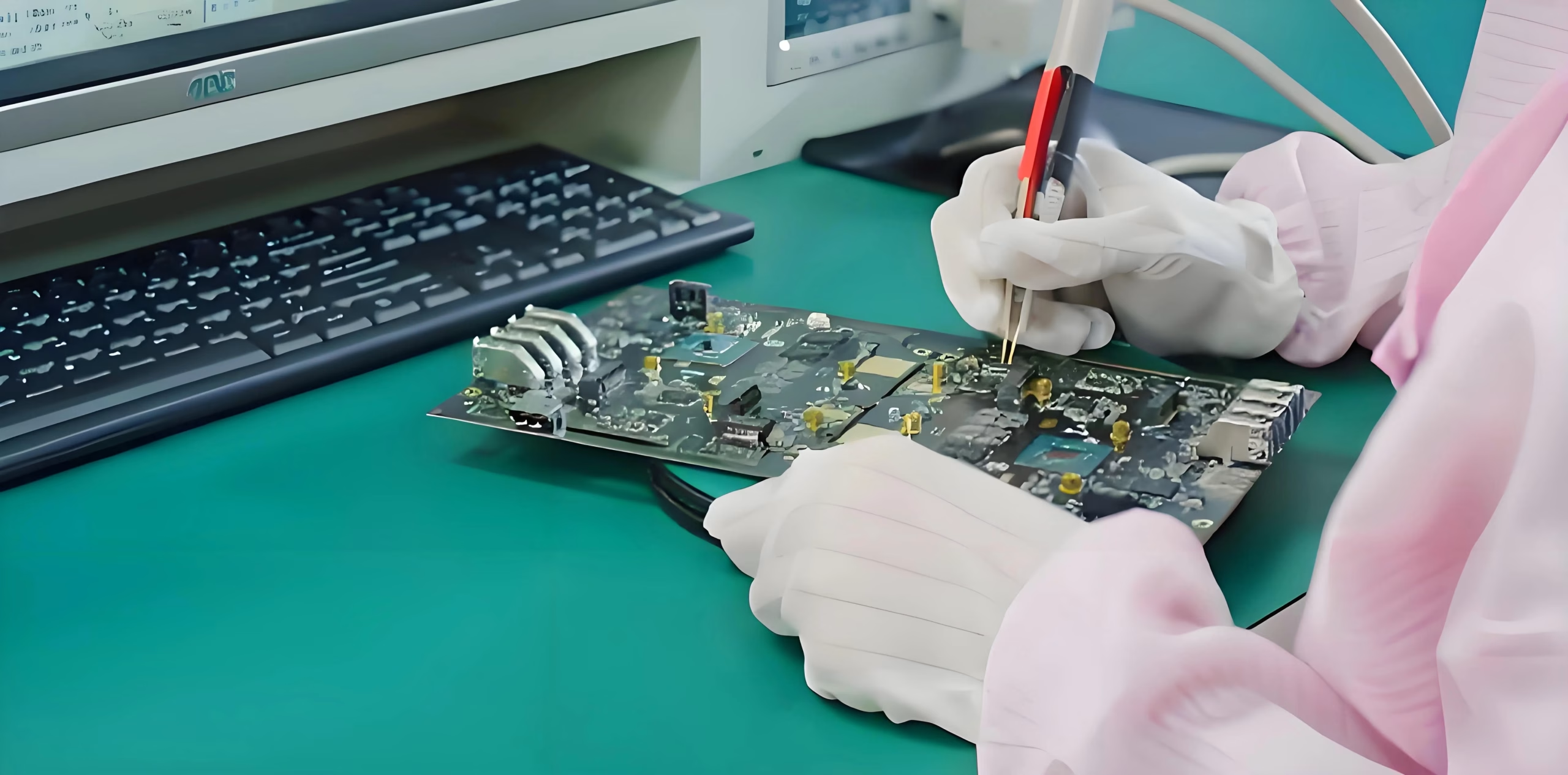
To ensure consistent quality and reliability across the electronics manufacturing industry, international standards play a crucial role. For Solder Paste Inspection, the guidelines established by IPC(Association Connecting Electronics Industries) are paramount. Specifically, IPC-A-610, “Acceptability of Electronic Assemblies”, and J-STD-001, “Requirements for Soldered Electrical and Electronic Assemblies”, provide detailed criteria for acceptable solder joint quality, which directly informs the pass/fail thresholds for SPI systems.
These standards define acceptable limits for solder paste volume, area, and registration for various component types and classes of electronic products. Adhering to these IPC standards allows manufacturers to set their SPI machine’s tolerance levels appropriately, ensuring that only boards meeting specified quality benchmarks proceed through the assembly process. This standardization is vital for achieving repeatable results and maintaining high levels of product reliability, regardless of the manufacturing location.
7. Integrating SPI for Optimal Process Control and DFM
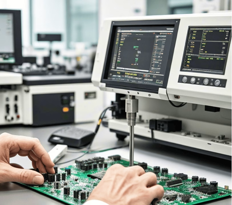
The true power of SPI extends beyond mere defect detection; it serves as a cornerstone for advanced process control and Design for Manufacturability(DFM) in SMT lines. Modern SPI systems are not isolated inspection units; they are integrated components of a smart factory ecosystem.
- Closed-Loop Process Control:SPI machines can provide real-time feedback to the upstream solder paste printer. If a trend of insufficient paste volume is detected, the SPI system can alert the printer to adjust parameters like squeegee pressure, speed, or stencil cleaning frequency. This automated feedback loop prevents recurring defects and maintains optimal printing conditions.
- Data-Driven Optimization:SPI generates a wealth of data on every solder paste deposit. This data can be analyzed to identify long-term trends, pinpoint specific problematic pads, or evaluate the performance of different stencil designs or solder paste types. This insight is invaluable for continuous process improvement.
- Design for Manufacturability(DFM): The data from SPI can also inform PCB design. If certain pad geometries or component types consistently show paste application issues, designers can adjust future layouts to optimize printability. DFM principles applied with SPI feedback ensure that designs are not only functional but also efficiently manufacturable, reducing potential defects from the outset.
- Industry 4.0 Traceability:Integrated SPI systems contribute to full product traceability, a key aspect of Industry 4.0. Each inspection result can be linked to a specific board, batch, and even individual components, providing a complete quality history. This is invaluable for quality audits, root cause analysis, and product recalls.
8. SPI vs. AOI: Complementary Guardians of Quality
While Solder Paste Inspection(SPI) is crucial, it’s often confused with Automated Optical Inspection(AOI). It’s important to understand that these technologies are complementary, each playing a distinct yet equally vital role in ensuring quality within the PCB assembly process.
- SPI(Solder Paste Inspection):Operates before component placement and reflow. Its sole focus is the quality and accuracy of the solder paste deposits. SPI confirms that the right amount of paste is in the right place, crucial for preventing 80-90% of SMT defects.
- AOI(Automated Optical Inspection):Typically operates after component placement(pre-reflow AOI) and/or after reflow soldering(post-reflow AOI). AOI inspects for component presence, correct placement, polarity, and post-reflow solder joint integrity(e.g., opens, shorts, component shift, tombstoning).
Together, SPI and AOI form a comprehensive quality backbone for SMT assembly lines, providing closed -loop process control that catches defects at their source, enables immediate corrective action, and generates the data needed for continuous process improvement.
9. Benefits of Advanced SPI Systems
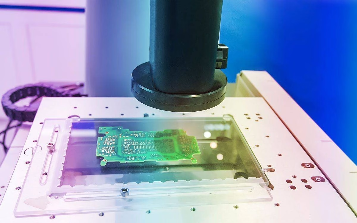
Investing in advanced 3D SPI systems offers substantial benefits to modern electronics manufacturers:
- Superior Defect Prevention:Catches critical flaws like insufficient or excessive paste, which are difficult to detect otherwise, before they become expensive problems. Prevents up to 70% of potential PCB defects.
- Enhanced Yield and Throughput:By reducing rework and scrap, production lines operate more efficiently, leading to higher output.
- Reduced Rework Costs:Addressing defects at the paste stage is significantly cheaper and less time-consuming than after reflow.
- Improved Product Quality and Reliability:Ensures consistently strong and reliable solder joints, enhancing the lifespan and performance of the final product.
- Data-Driven Decision Making:Provides rich data for process monitoring, analysis, and continuous improvement, supporting Industry 4.0 initiatives.
- Support for Miniaturization:Essential for handling the increasing complexity and miniaturization of components, such as 0201 packages and fine-pitch ICs, where paste deposition precision is paramount.
10. Solder Paste Inspection FAQs
Question 1: What is the main difference between 2D and 3D SPI?
2D SPI can only measure the area and presence of solder paste, lacking crucial height information. 3D SPI, however, uses structured light to accurately measure volume, height, area, and shape, providing a comprehensive topographical view of the paste deposit, which is critical for preventing common defects.
Question 2: Where is SPI typically placed in the SMT assembly line?
SPI is strategically placed immediately after the solder paste printer and before the component placement(pick-and-place) machine. This allows for immediate detection and correction of printing defects before components are committed to the board.
Question 3: How much can SPI reduce defects in PCB assembly?
Solder Paste Inspection is incredibly effective, preventing up to 70% of potential PCB defects that originate from the solder paste printing process. Given that 80-90% of SMT defects stem from this stage, SPI’s role is critical in defect reduction.
11. Summary
Solder Paste Inspection(SPI) is an indispensable quality control measure in modern PCB assembly, particularly within SMT processes. By meticulously inspecting the volume, area, height, and alignment of solder paste deposits immediately after printing, SPI proactively addresses the root cause of the majority of SMT defects. This early detection capability translates directly into significant cost savings by minimizing rework, increasing manufacturing yield, and enhancing overall product reliability. Leveraging advanced 3D technology, SPI systems provide critical data for closed-loop process control, supporting DFM initiatives and integrating seamlessly into Industry 4.0 environments. For any manufacturer striving for zero-defect production and robust, high-performance electronics, SPI is not just an option, but a fundamental requirement.
Key Takeaways
- SPI prevents up to 70% of PCB defects by inspecting solder paste before component placement.
- The majority(80-90%) of SMT defects originate from the solder paste printing process.
- Early defect detection via SPI significantly reduces rework costs, which can be 10-100 times higher if defects are found later.
- Modern SPI uses 3D technology to accurately measure volume, height, area, and alignment of solder paste.
- SPI provides crucial data for closed-loop process control and Design for Manufacturability(DFM).
- SPI and AOI are complementary technologies, with SPI focusing on paste quality and AOI on component placement and post-reflow solder joints.
OrinewPCB has focused as a one-stop PCB assembly manufacturer from PCB Manufacturing to Electronic Components Sourcing to PCB Assembly to Test to Program IC for more than 14 Years with reliable quality and fastest delivery for global clients.
Contact Us
Phone: +86-18123905375
Email: sales@assemblepcb.com
WhatsApp: +86-18123905375
Wechat: +86-18123905375
Free Queto
Latest Blog


Table Of Contents
Contact Us
Phone: +86-18123905375
Email: sales@assemblepcb.com
WhatsApp: +86-18123905375
Wechat: +86-18123905375
Free Queto
