
Solder Paste Printing for SMT: Stencil Thickness, Apertures, and Defect Troubleshooting
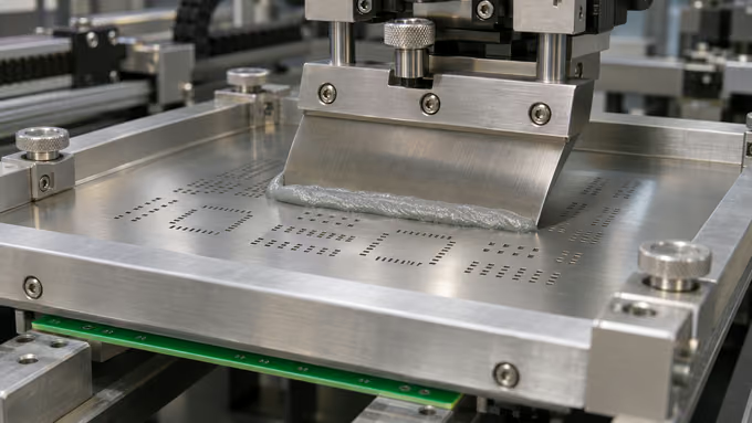
Table Of Contents
Cover image: Generated illustration of the squeegee and paste roll during stencil printing.
Start with the smallest critical stencil aperture, then verify paste volume on both the smallest and largest deposits. A thicker stencil holds more paste, but a small opening can release a smaller share of it. For solder paste printing on a mixed SMT board, use the area ratio to screen the stencil design and first-print solder paste inspection (SPI) to validate what actually lands on the pads.
How Solder Paste Printing Works in SMT
In SMT stencil printing, the printer aligns a perforated metal foil to the bare PCB. The board support and clamps hold the PCB flat so the foil can seal against the board around the apertures. A squeegee rolls paste across the foil, fills the openings, and wipes the top surface. The board then separates from the foil, leaving deposits on the pads for inspection and placement.
Pressure, print speed, blade condition, separation settings, paste condition, and underside cleaning interact. A change in pressure can mask poor board support for a few prints. Start by confirming the stencil revision, the alignment, and the support before tuning the printer. Use the paste supplier’s handling instructions and your assembler’s qualified recipe as starting conditions.
Calculate the Stencil Aperture Area Ratio
Area ratio compares the area of the opening at the board face with the area of the aperture walls. It is a geometry check for paste release. For a straight-walled rectangular opening with length L, width W, and local foil thickness t, use the same units throughout.
Area ratio = L × W ÷ [2 × (L + W) × t]
Nominal aperture volume = L × W × t
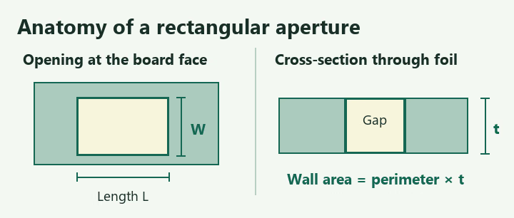
For a straight-walled circular opening, the area ratio simplifies to D ÷ (4 × t), where D is the diameter. Use foil supplier data or the actual aperture geometry for rounded, tapered, or irregular openings. For stepped foils, use the thickness at the specific aperture.
Area ratio and transfer efficiency measure different things
About 0.66 is a practical screening value for conventional stencil design. Apertures near or below it warrant a release review with the stencil and paste suppliers. Wall finish, paste formulation and powder size, and the release conditions can change print results at the same ratio. Texas Instruments discusses challenging area ratios in its QFN and SON attachment guide, and Indium reports measured differences in its ultrafine aperture printing experiment.
Transfer efficiency = measured deposit volume ÷ nominal aperture volume × 100%. Use the final aperture geometry for the denominator and a measured SPI volume for the numerator. Check what your SPI software uses as its volume reference before treating the displayed percentage as transfer efficiency. Review variation across equivalent pads and successive prints alongside the average.
Choose SMT Stencil Thickness for a Mixed Board
Consider a hypothetical board with a fine-pitch QFN and a larger surface-mount connector. The released stencil drawing proposes a 0.24 × 0.30 mm opening for one QFN perimeter pad and a 1.20 × 1.50 mm opening for one connector pad. Compare two uniform foils before ordering the stencil. The dimensions below illustrate the calculation and should be checked against the actual package and land pattern on a real build.
| Foil thickness | QFN area ratio | QFN volume | Connector area ratio | Connector volume |
|---|---|---|---|---|
| 100 µm | 0.667 | 0.00720 mm³ | 3.33 | 0.180 mm³ |
| 125 µm | 0.533 | 0.00900 mm³ | 2.67 | 0.225 mm³ |
At 100 µm, the small opening is just above the screening value, so it deserves pilot verification. At 125 µm, the same opening carries 25% more nominal volume while its area ratio drops to 0.533. If SPI measured 0.00576 mm³ with the thinner foil and 0.00540 mm³ with the thicker foil, the calculated transfer efficiencies would be 80% and 60%. These are illustrative readings. They show how a larger aperture volume can yield a smaller deposit when release deteriorates.
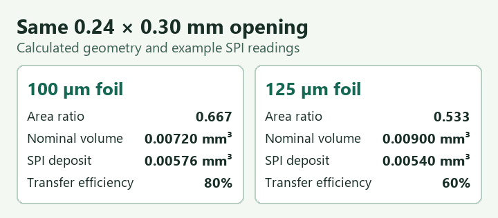
When the thin foil leaves a large pad short
Start by asking whether the connector actually needs more solder at its critical terminals or anchors, based on the package guidance and pilot joints. If it does, review a local aperture adjustment with adequate spacing and containment. When the two regions still need different volumes, ask the stencil supplier to review a step stencil. Confirm where the thickness transition can sit relative to nearby apertures, the squeegee path, and stencil wiping.
Review the QFN exposed pad separately. The device manufacturer may recommend multiple paste windows to control deposit volume and provide paths for flux outgassing. Use the component’s documentation and inspect the finished joint as required. The area covered by the apertures, the measured paste transfer, and the post-reflow void percentage are three separate measurements.
Verify the First Print Before Placement
- Match the files to the job. Compare board and stencil revisions, panel orientation, paste layers, fiducials, and critical apertures. Record the stencil ID, paste lot, and printer recipe.
- Print on supported hardware. Check that the board is flat and aligned. Verify paste conditioning and any restart procedure against the supplier instructions and the approved process.
- Read the SPI evidence. Measure volume and offset on fine-pitch leads, large terminals, and critical sites near panel edges. Compare equivalent pads at multiple panel positions. If both squeegee directions are used, verify both.
- Recheck after a change. Confirm repeatability across consecutive prints and after a planned pause or wipe. Log each change with the pad IDs and measurements that justify accepting it.
Agree on pad-specific acceptance criteria with the assembler. A board-wide average can hide an individual QFN lead with a repeatable low deposit. See the AssemblePCB guide to solder paste inspection for what SPI measures and where it fits in production.
Troubleshoot Solder Paste Printing Defects
Find the first stage where the defect is visible. Compare the same reference designator and pad location in the SPI record, any pre-reflow placement evidence, and the finished-board inspection. A bridge seen before placement points you toward the print. A bridge absent from SPI and visible after placement makes component alignment or paste squeeze-out worth checking.
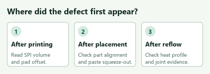
| Pattern | First checks | How to verify |
|---|---|---|
| One small opening repeatedly prints low | Check for a partial blockage, low area ratio, or damage at the aperture wall. | Inspect the aperture, follow the approved cleaning procedure, and compare successive SPI readings at that location. |
| Low or smeared deposits cluster near one panel edge | Review support, board flatness, clamping, and the stencil-to-board seal. | Compare the affected panel positions with an equivalent pad at the center after correcting support. |
| Deposits shift in the same direction | Check fiducial recognition, panel orientation, and registration. Look for a pattern by stroke direction. | Compare X and Y offsets by panel position and stroke direction before and after alignment correction. |
| Adjacent deposits touch before placement | Inspect underside contamination, aperture spacing, board support, and signs of paste spreading. | Inspect after an approved wipe and measure SPI offset and volume at the affected pad pair. |
| SPI is in limits, but a bridge or open appears downstream | Review placement position and force, component and board geometry, and the measured reflow profile. | Compare stage-by-stage evidence at that reference designator and use X-ray where appropriate for hidden joints. |
When diagnosing a repeat defect, isolate affected boards and change one variable at a time unless a planned experiment calls for multiple factors. Keep the initial SPI record and follow the approved cleaning and reprint procedure before trying another print on a failed board.
Frequently Asked Questions
Is a 100 µm or 125 µm stencil better for fine-pitch SMT?
Calculate the area ratio of the smallest critical apertures for both, then confirm deposits at the low- and high-volume ends of the design. The better choice produces the required volume with repeatable prints on both groups.
Should I use finer solder paste powder for small openings?
Finer powder can improve transfer in some small openings. Use the stencil supplier’s aperture recommendations and the paste supplier’s data, then qualify the paste on the actual board, including its behavior after a pause.
What should I send for a stencil review?
Send the relevant paste layer, board and panel revisions, and the part numbers and package drawings for the smallest openings and the largest critical deposits. If you have an existing stencil, include its local foil thickness, the aperture drawing, and SPI readings for the affected pads.
Technical References
- Pan and colleagues on aperture geometry, foil thickness, and paste transfer
- Texas Instruments application note on QFN and SON attachment
- Indium Corporation experiment on ultrafine aperture printing
Request a Stencil and First-Print Review
For repeatable solder paste printing, screen the smallest critical aperture, verify enough paste on the large joints, and record what the first prints show before placement. If the two volume requirements conflict, bring the actual aperture drawing and package requirements into the stencil review.
Send AssemblePCB the board revision, paste layer, batch quantity, and critical component references. Flag the smallest opening and any connector or exposed pad that needs special review. Include SPI measurements or defect photos if the board has already been built.
Contact Us
Phone: +86-18123905375
Email: sales@assemblepcb.com
WhatsApp: +86-18123905375
Wechat: +86-18123905375
Free Queto
Latest Blog
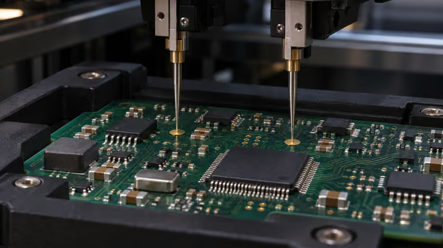

Table Of Contents
Contact Us
Phone: +86-18123905375
Email: sales@assemblepcb.com
WhatsApp: +86-18123905375
Wechat: +86-18123905375
Free Queto
